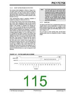
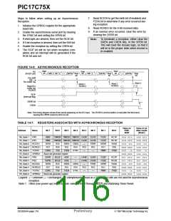
PIC17C75X
tion). The TX/CK pin will remain an output if the CSRC
bit is set (internal clock). The transmitter logic is not
reset, although it is disconnected from the pins. In order
to reset the transmitter, the user has to clear the TXEN
bit. If the SREN bit is set (to interrupt an ongoing trans-
mission and receive a single word), then after the sin-
gle word is received, SREN will be cleared and the
serial port will revert back to transmitting, since the
TXEN bit is still set.The DT line will immediately switch
from hi-impedance receive mode to transmit and start
driving. To avoid this, TXEN should be cleared.
14.3
USART Synchronous Master Mode
In Master Synchronous mode, the data is transmitted in
a half-duplex manner; i.e. transmission and reception
do not occur at the same time: when transmitting data,
the reception is inhibited and vice versa. The synchro-
nous mode is entered by setting the SYNC
(TXSTA<4>) bit. In addition, the SPEN (RCSTA<7>)
bit is set in order to configure the I/O pins to CK (clock)
and DT (data) lines respectively. The Master mode
indicates that the processor transmits the master clock
on the CK line. The Master mode is entered by setting
the CSRC (TXSTA<7>) bit.
In order to select 9-bit transmission, the
TX9 (TXSTA<6>) bit should be set and the ninth bit
should be written to TX9D (TXSTA<0>). The ninth bit
must be written before writing the 8-bit data to TXREG.
This is because a data write to TXREG can result in an
immediate transfer of the data to the TSR (if the TSR is
empty). If the TSR was empty and TXREG was written
before writing the “new” TX9D, the “present” value of
TX9D is loaded.
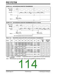
14.3.1 USART SYNCHRONOUS MASTER
TRANSMISSION
The USART transmitter block diagram is shown in
Figure 14-3. The heart of the transmitter is the transmit
(serial) shift register (TSR).The shift register obtains its
data from the read/write transmit buffer TXREG.
TXREG is loaded with data in software. The TSR is not
loaded until the last bit has been transmitted from the
previous load. As soon as the last bit is transmitted, the
TSR is loaded with new data from TXREG (if available).
Once TXREG transfers the data to the TSR (occurs in
one TCY at the end of the current BRG cycle), TXREG
is empty and the TXIF bit is set. This interrupt can be
enabled/disabled by setting/clearing the TXIE bit. TXIF
will be set regardless of the state of bit TXIE and cannot
be cleared in software. It will reset only when new data
is loaded into TXREG. While TXIF indicates the status
of TXREG, TRMT (TXSTA<1>) shows the status of the
TSR. TRMT is a read only bit which is set when the
TSR is empty. No interrupt logic is tied to this bit, so the
user has to poll this bit in order to determine if the TSR
is empty. The TSR is not mapped in data memory, so it
is not available to the user.
Steps to follow when setting up a Synchronous Master
Transmission:
1. Initialize the SPBRG register for the appropriate
baud rate (see Baud Rate Generator Section for
details).
2. Enable the synchronous master serial port by
setting the SYNC, SPEN, and CSRC bits.
3. Ensure that the CREN and SREN bits are clear
(these bits override transmission when set).
4. If interrupts are desired, then set the TXIE bit
(the GLINTD bit must be clear and the PEIE bit
must be set).
5. If 9-bit transmission is desired, then set the TX9
bit.
6. Start transmission by loading data to the
TXREG register.
Transmission is enabled by setting the TXEN
(TXSTA<5>) bit. The actual transmission will not occur
until TXREG has been loaded with data. The first data
bit will be shifted out on the next available rising edge
of the clock on the TX/CK pin. Data out is stable around
the falling edge of the synchronous clock
(Figure 14-10). The transmission can also be started
by first loading TXREG and then setting TXEN. This is
advantageous when slow baud rates are selected,
since BRG is kept in RESET when the TXEN, CREN,
and SREN bits are clear. Setting the TXEN bit will start
the BRG, creating a shift clock immediately. Normally
when transmission is first started, the TSR is empty, so
a transfer to TXREG will result in an immediate transfer
to the TSR, resulting in an empty TXREG.
Back-to-back transfers are possible.
7. If 9-bit transmission is selected, the ninth bit
should be loaded in TX9D.
8. Enable the transmission by setting TXEN.
Writing the transmit data to the TXREG, then enabling
the transmit (setting TXEN) allows transmission to start
sooner than doing these two events in the reverse
order.
Note: To terminate a transmission, either clear
the SPEN bit, or the TXEN bit. This will
reset the transmit logic, so that it will be in
the proper state when transmit is
re-enabled.
Clearing TXEN during a transmission will cause the
transmission to be aborted and will reset the transmit-
ter. The RX/DT and TX/CK pins will revert to hi-imped-
ance. If either CREN or SREN are set during a
transmission, the transmission is aborted and the
RX/DT pin reverts to a hi-impedance state (for a recep-
1997 Microchip Technology Inc.
Preliminary
DS30264A-page 117

 MICROCHIP [ MICROCHIP ]