PIC17C75X
14.2.2 USART ASYNCHRONOUS RECEIVER
Note: The FERR and the 9th receive bit are buff-
ered the same way as the receive data.
Reading the RCREG register will allow the
RX9D and FERR bits to be loaded with val-
ues for the next received Received data.
Therefore, it is essential for the user to
read the RCSTA register before reading
RCREG in order not to lose the old FERR
and RX9D information.
The receiver block diagram is shown in Figure 14-4.
The data comes in the RX/DT pin and drives the data
recovery block. The data recovery block is actually a
high speed shifter operating at 16 times the baud rate,
whereas the main receive serial shifter operates at the
bit rate or at FOSC.
Once asynchronous mode is selected, reception is
enabled by setting bit CREN (RCSTA<4>).
The heart of the receiver is the receive (serial) shift reg-
ister (RSR). After sampling the stop bit, the received
data in the RSR is transferred to the RCREG (if it is
empty). If the transfer is complete, the interrupt bit,
RCIF, is set. The actual interrupt can be enabled/dis-
abled by setting/clearing the RCIE bit. RCIF is a read
only bit which is cleared by the hardware. It is cleared
when RCREG has been read and is empty. RCREG is
a double buffered register; (i.e. it is a two deep FIFO).
It is possible for two bytes of data to be received and
transferred to the RCREG FIFO and a third byte begin
shifting to the RSR. On detection of the stop bit of the
third byte, if the RCREG is still full, then the overrun
error bit, OERR (RCSTA<1>) will be set. The word in
the RSR will be lost. RCREG can be read twice to
retrieve the two bytes in the FIFO.The OERR bit has to
be cleared in software which is done by resetting the
receive logic (CREN is set). If the OERR bit is set,
transfers from the RSR to RCREG are inhibited, so it is
essential to clear the OERR bit if it is set. The framing
error bit FERR (RCSTA<2>) is set if a stop bit is not
detected.
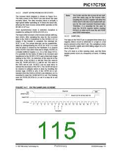
14.2.3 SAMPLING
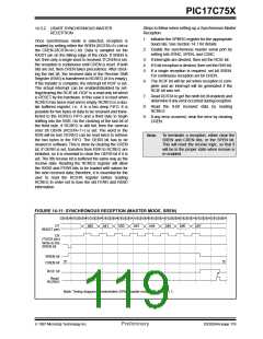
The data on the RX/DT pin is sampled three times by a
majority detect circuit to determine if a high or a low
level is present at the RX/DT pin.The sampling is done
on the seventh, eighth and ninth falling edges of a x16
clock (Figure 14-7).
The x16 clock is a free running clock, and the three
sample points occur at a frequency of every 16 falling
edges.
FIGURE 14-7: RX PIN SAMPLING SCHEME
Start bit
Bit0
RX
(RX/DT pin)
Baud CLK for all but start bit
baud CLK
x16 CLK
1
2
3
4
5
6
7
8
9
10 11 12 13 14 15 16
1
2
3
Samples
1997 Microchip Technology Inc.
Preliminary
DS30264A-page 115

 MICROCHIP [ MICROCHIP ]