PIC17C75X
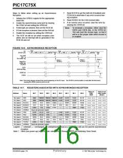
Steps to follow when setting up an Asynchronous
Reception:
7. Read RCSTA to get the ninth bit (if enabled) and
FERR bit to determine if any error occurred dur-
ing reception.
1. Initialize the SPBRG register for the appropriate
baud rate.
8. Read RCREG for the 8-bit received data.
9. If an overrun error occurred, clear the error by
clearing the OERR bit.
2. Enable the asynchronous serial port by clearing
the SYNC bit and setting the SPEN bit.
3. If interrupts are desired, then set the RCIE bit.
4. If 9-bit reception is desired, then set the RX9 bit.
5. Enable the reception by setting the CREN bit.
Note: To terminate a reception, either clear the
SREN and CREN bits, or the SPEN bit.
This will reset the receive logic, so that it
will be in the proper state when receive is
re-enabled.
6. The RCIF bit will be set when reception com-
pletes and an interrupt will be generated if the
RCIE bit was set.
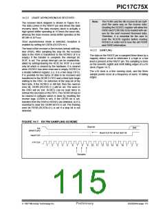
FIGURE 14-8: ASYNCHRONOUS RECEPTION
Start
RX
Start
bit
Start
bit
bit
bit0
bit1
Stop
bit
Stop
bit
bit7/8 Stop
bit
bit0
bit7/8
bit7/8
(RX/DT pin)
Rcv shift
reg
Rcv buffer reg
Word 3
Word 2
RCREG
Word 1
RCREG
Read Rcv
buffer reg
RCREG
RCIF
(interrupt flag)
OERR bit
CREN
Note: This timing diagram shows three words appearing on the RX input. The RCREG (receive buffer) is read after the third word,
causing the OERR (overrun) bit to be set.
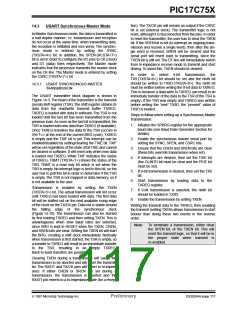
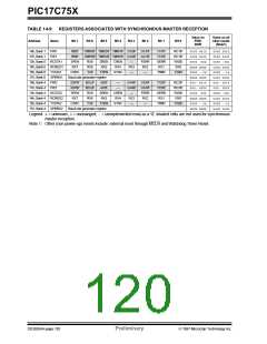
TABLE 14-7: REGISTERS ASSOCIATED WITH ASYNCHRONOUS RECEPTION
Value on
POR,
BOR
Value on all
other resets
(Note1)
Address
Name
Bit 7
Bit 6
Bit 5
Bit 4
Bit 3
Bit 2
Bit 1
Bit 0
16h, Bank 1
17h, Bank 1
13h, Bank 0
14h, Bank 0
15h, Bank 0
17h, Bank 0
10h, Bank 4
11h, Bank 4
13h, Bank 4
14h, Bank 4
15h, Bank 4
17h, Bank 4
PIR1
RBIF
RBIE
SPEN
RX7
TMR3IF TMR2IF TMR1IF CA2IF
TMR3IE TMR2IE TMR1IE CA2IE
CA1IF
CA1IE
FERR
RX2
TX1IF
TX1IE
OERR
RX1
RC1IF
RC1IE
RX9D
RX0
0000 0010
0000 0000
0000 -00x
xxxx xxxx
0000 --1x
xxxx xxxx
000- 0010
000- 0000
0000 -00x
xxxx xxxx
0000 --1x
xxxx xxxx
0000 0010
0000 0000
0000 -00u
uuuu uuuu
0000 --1u
uuuu uuuu
000- 0010
000- 0000
0000 -00u
uuuu uuuu
0000 --1u
uuuu uuuu
PIE1
RCSTA1
RCREG1
TXSTA1
SPBRG1
PIR2
RX9
RX6
TX9
SREN
RX5
CREN
RX4
—
RX3
—
CSRC
TXEN
SYNC
—
TRMT
TX9D
Baud rate generator register
SSPIF
SSPIE
SPEN
RX7
BCLIF
BCLIE
RX9
ADIF
ADIE
SREN
RX5
—
—
CA4IF
CA4IE
—
CA3IF
CA3IE
FERR
RX2
TX2IF
TX2IE
OERR
RX1
RC2IF
RC2IE
RX9D
RX0
PIE2
RCSTA2
RCREG2
TXSTA2
SPBRG2
CREN
RX4
SYNC
RX6
RX3
—
CSRC
TX9
TXEN
—
TRMT
TX9D
Baud rate generator register
Legend: x= unknown, u= unchanged, -= unimplemented read as a '0', shaded cells are not used for asynchronous
reception.
Note 1: Other (non power-up) resets include: external reset through MCLR and Watchdog Timer Reset.
DS30264A-page 116
Preliminary
1997 Microchip Technology Inc.

 MICROCHIP [ MICROCHIP ]