PIC16F913/914/916/917/946
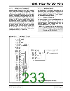
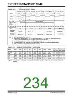
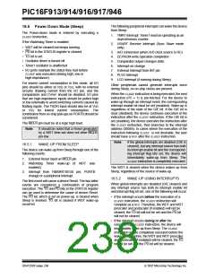
FIGURE 16-8:
INT PIN INTERRUPT TIMING
Q1 Q2 Q3 Q4 Q1 Q2 Q3 Q4 Q1 Q2 Q3 Q4 Q1 Q2 Q3 Q4 Q1 Q2 Q3 Q4
OSC1
(3)
CLKOUT
(4)
INT pin
(1)
(1)
(2)
(5)
Interrupt Latency
INTF Flag
(INTCON reg.)
GIE bit
(INTCON reg.)
Instruction Flow
PC
0004h
PC + 1
PC + 1
—
0005h
PC
Instruction
Fetched
Inst (PC)
Inst (PC + 1)
Inst (0004h)
Inst (0005h)
Inst (0004h)
Instruction
Executed
Dummy Cycle
Dummy Cycle
Inst (PC)
Inst (PC - 1)
Note 1: INTF flag is sampled here (every Q1).
2: Asynchronous interrupt latency = 3-4 TCY. Synchronous latency = 3 TCY, where TCY = instruction cycle time.
Latency is the same whether Inst (PC) is a single cycle or a 2-cycle instruction.
3: CLKOUT is available only in INTOSC and RC Oscillator modes.
4: For minimum width of INT pulse, refer to AC specifications in Section 19.0 “Electrical Specifications”.
5: INTF is enabled to be set any time during the Q4-Q1 cycles.
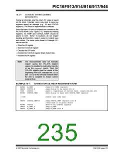
TABLE 16-6: SUMMARY OF INTERRUPT REGISTERS
Value on
POR, BOR other Resets
Value on all
Name
Bit 7
Bit 6
Bit 5
Bit 4
Bit 3
Bit 2
Bit 1
Bit 0
INTCON
PIR1
GIE
EEIF
PEIE
ADIF
C2IF
ADIE
C2IE
T0IE
RCIF
C1IF
RCIE
C1IE
INTE
TXIF
RBIE
SSPIF
—
T0IF
INTF
RBIF
0000 000x 0000 000x
CCP1IF TMR2IF TMR1IF 0000 0000 0000 0000
LVDIF CCP2IF 0000 -0-0 0000 -0-0
CCP1IE TMR2IE TMR1IE 0000 0000 0000 0000
LVDIE CCP2IE 0000 -0-0 0000 -0-0
PIR2
OSFIF
EEIE
LCDIF
TXIE
—
PIE1
SSPIE
—
PIE2
OSFIE
LCDIE
—
Legend:
x= unknown, u= unchanged, -= unimplemented locations read as ‘0’. Shaded cells are not used by the Interrupt
Module.
DS41250F-page 232
© 2007 Microchip Technology Inc.

 MICROCHIP [ MICROCHIP ]