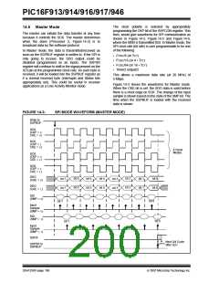
PIC16F913/914/916/917/946
The SSPCON register allows control of the I2C
2
14.11 SSP I C Operation
operation. Four mode selection bits (SSPCON<3:0>)
The SSP module in I2C mode, fully implements all slave
functions, except general call support, and provides
interrupts on Start and Stop bits in hardware to facilitate
firmware implementations of the master functions. The
SSP module implements the Standard mode
specifications, as well as 7-bit and 10-bit addressing.
allow one of the following I2C modes to be selected:
• I2C Slave mode (7-bit address)
• I2C Slave mode (10-bit address)
• I2C Slave mode (7-bit address), with Start and
Stop bit interrupts enabled to support Firmware
Master mode
• I2C Slave mode (10-bit address), with Start and
Stop bit interrupts enabled to support Firmware
Master mode
• I2C Start and Stop bit interrupts enabled to
support Firmware Master mode; Slave is idle
Two pins are used for data transfer. These are the
RC6/TX/CK/SCK/SCL/SEG9 pin, which is the clock
(SCL), and the RC7/RX/DT/SDI/SDA/SEG8 pin, which
is the data (SDA).
The SSP module functions are enabled by setting SSP
enable bit SSPEN (SSPCON<5>).
Selection of any I2C mode with the SSPEN bit set
forces the SCL and SDA pins to be open drain,
provided these pins are programmed to inputs by
setting the appropriate TRISC bits. Pull-up resistors
must be provided externally to the SCL and SDA pins
for proper operation of the I2C module.
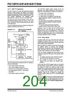
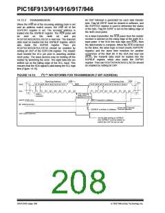
FIGURE 14-7:
SSP BLOCK DIAGRAM
(I2C™ MODE)
Internal
Data Bus
Read
Write
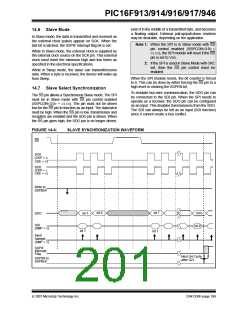
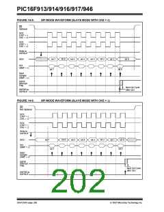
14.12 Slave Mode
SCK/
SCL
SSPBUF Reg
In Slave mode, the SCL and SDA pins must be
configured as inputs (TRISC<7,6> are set). The SSP
module will override the input state with the output data
when required (slave-transmitter).
Shift
Clock
SSPSR Reg
When an address is matched, or the data transfer after
an address match is received, the hardware
automatically will generate the Acknowledge (ACK)
pulse, and then load the SSPBUF register with the
received value currently in the SSPSR register.
SDI/
SDA
MSb
LSb
Addr Match
Match Detect
There are certain conditions that will cause the SSP
module not to give this ACK pulse. They include (either
or both):
SSPADD Reg
Set, Reset
S, P bits
(SSPSTAT Reg.)
Start and
Stop bit Detect
a) The Buffer Full bit BF of the SSPSTAT register
was set before the transfer was received.
b) The overflow bit SSPOV of the SSPCON
register was set before the transfer was
received.
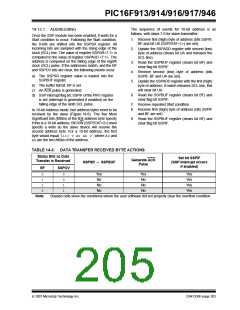
The SSP module has five registers for the I2C operation,
which are listed below.
In this case, the SSPSR register value is not loaded
into the SSPBUF, but bit SSPIF of the PIR1 register is
set. Table 14-3 shows the results of when a data
transfer byte is received, given the status of bits BF and
SSPOV. The shaded cells show the condition where
user software did not properly clear the overflow
condition. Flag bit BF is cleared by reading the
SSPBUF register, while bit SSPOV is cleared through
software.
• SSP Control register (SSPCON)
• SSP STATUS register (SSPSTAT)
• Serial Receive/Transmit Buffer (SSPBUF)
• SSP Shift register (SSPSR) – Not directly
accessible
• SSP Address register (SSPADD)
The SCL clock input must have a minimum high and low
for proper operation. For high and low times of the I2C
specification, as well as the requirements of the SSP
module, see Section 19.0 “Electrical Specifications”.
DS41250F-page 202
© 2007 Microchip Technology Inc.

 MICROCHIP [ MICROCHIP ]