PIC16F87/88
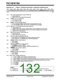
REGISTER 15-1: CONFIG1: CONFIGURATION WORD 1 REGISTER (ADDRESS 2007h)
R/P-1 R/P-1 R/P-1 R/P-1 R/P-1 R/P-1 R/P-1 R/P-1 R/P-1 R/P-1
CP CCPMX RESV WRT1 WRT0 CPD LVP BOREN MCLRE FOSC2 PWRTEN WDTEN FOSC1 FOSC0
bit 13 bit 0
R/P-1
R/P-1 R/P-1 R/P-1
bit 13
bit 12
bit 11
CP: FLASH Program Memory Code Protection bits
1= Code protection off
0= 0000h to 0FFFh code protected (All protected)
CCPMX: CCP1 Pin Selection bit
1= CCP1 function on RB0
0= CCP1 function on RB3
DEBUG: In-Circuit Debugger Mode bit
1= In-circuit debugger disabled, RB6 and RB7 are general purpose I/O pins
0= In-circuit debugger enabled, RB6 and RB7 are dedicated to the debugger
bit 10-9 WRT<1:0>: FLASH Program Memory Write Enable bits
11= Write protection off
10= 0000h to 00FFh write protected, 0100h to 0FFFh may be modified by EECON control
01= 0000h to 07FFh write protected, 0800h to 0FFFh may be modified by EECON control
00= 0000h to 0FFFh write protected
bit 8
bit 7
bit 6
bit 5
bit 3
bit 2
CPD: Data EE Memory Code Protection bit
1= Code protection off
0= Data EE memory code protected
LVP: Low-Voltage Programming Enable bit
1= RB3/PGM pin has PGM function, low-voltage programming enabled
0= RB3 is digital I/O, HV on MCLR must be used for programming
BOREN: Brown-out Reset Enable bit
1= BOR enabled
0= BOR disabled
MCLRE: RA5/MCLR Pin Function Select bit
1= RA5/MCLR pin function is MCLR
0= RA5/MCLR pin function is digital I/O, MCLR internally tied to VDD
PWRTEN: Power-up Timer Enable bit
1= PWRT disabled
0= PWRT enabled
WDTEN: Watchdog Timer Enable bit
1= WDT enabled
0= WDT disabled
bit 4, 1-0 FOSC<2:0>: Oscillator Selection bits
111= EXTRC oscillator; CLKO function on RA6/OSC2/CLKO
110= EXTRC oscillator; port I/O function on RA6/OSC2/CLKO
101= INTRC oscillator; CLKO function on RA6/OSC2/CLKO pin and port I/O function on RA7/OSC1/CLKI pin
100= INTRC oscillator; port I/O function on both RA6/OSC2/CLKO pin and RA7/OSC1/CLKI pin
011= EXTCLK; port I/O function on RA6/OSC2/CLKO
010= HS oscillator
001= XT oscillator
000= LP oscillator
Legend:
R = Readable bit
-n = Value at POR
W = Writable bit
‘1’ = Bit is set
U = Unimplemented bit, read as ‘0’
‘0’ = Bit is cleared x = Bit is unknown
DS30487B-page 130
Preliminary
2003 Microchip Technology Inc.

 MICROCHIP [ MICROCHIP ]