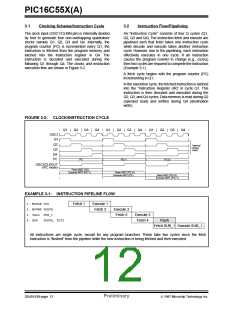
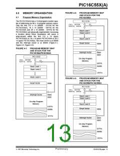
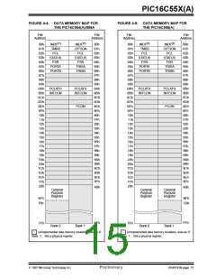
PIC16C55X(A)
4.2.2
SPECIAL FUNCTION REGISTERS
The special function registers can be classified into two
sets (core and peripheral). The special function regis-
ters associated with the “core” functions are described
in this section. Those related to the operation of the
peripheral features are described in the section of that
peripheral feature.
The special function registers are registers used by the
CPU and Peripheral functions for controlling the
desired operation of the device (Table 4-1). These
registers are static RAM.
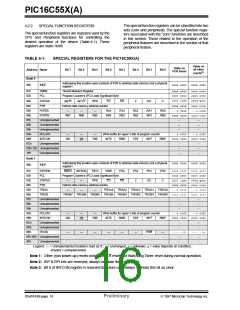
TABLE 4-1:
SPECIAL REGISTERS FOR THE PIC16C55X(A)
Value on
Value on
POR Reset
all other
resets(1)
Address Name
Bank 0
Bit 7
Bit 6
Bit 5
Bit 4
Bit 3
Bit 2
Bit 1
Bit 0
Addressing this location uses contents of FSR to address data memory (not a physical
register)
00h
INDF
xxxx xxxx
xxxx xxxx
01h
02h
03h
04h
05h
06h
07h
08h
09h
0Ah
0Bh
0Ch
TMR0
Timer0 Module’s Register
xxxx xxxx
0000 0000
0001 1xxx
uuuu uuuu
0000 0000
000q quuu
PCL
Program Counter's (PC) Least Significant Byte
IRP(2)
RP1(2)
STATUS
RP0
TO
PD
Z
DC
C
FSR
Indirect data memory address pointer
xxxx xxxx
uuuu uuuu
PORTA
—
—
—
RA4
RB4
RA3
RB3
RA2
RB2
RA1
RB1
RA0
RB0
---x xxxx
---u uuuu
PORTB
RB7
RB6
RB5
xxxx xxxx
uuuu uuuu
Unimplemented
Unimplemented
Unimplemented
PCLATH
—
—
—
—
—
—
—
—
—
Write buffer for upper 5 bits of program counter
INTE RBIE T0IF INTF
---0 0000
---0 0000
INTCON
GIE
(3)
T0IE
RBIF
0000 000x
0000 000x
Unimplemented
—
—
—
—
—
—
0Dh-1Eh Unimplemented
1Fh
Unimplemented
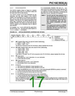
Bank 1
Addressing this location uses contents of FSR to address data memory (not a physical
register)
xxxx xxxx
xxxx xxxx
80h
INDF
81h
82h
83h
84h
85h
86h
87h
88h
89h
8Ah
8Bh
8Ch
8Dh
8Eh
OPTION
RBPU
Program Counter's (PC) Least Significant Byte
RP0 TO
Indirect data memory address pointer
TRISA4 TRISA3 TRISA2 TRISA1 TRISA0
TRISB7 TRISB6 TRISB5 TRISB4 TRISB3 TRISB2 TRISB1 TRISB0
INTEDG
T0CS
T0SE
PSA
PS2
PS1
PS0
1111 1111
1111 1111
PCL
0000 0000
0000 0000
STATUS
—
—
PD
Z
DC
C
0001 1xxx
000q quuu
FSR
xxxx xxxx
uuuu uuuu
TRISA
—
—
—
---1 1111
---1 1111
TRISB
1111 1111
1111 1111
Unimplemented
Unimplemented
Unimplemented
PCLATH
—
—
—
—
—
—
—
—
—
Write buffer for upper 5 bits of program counter
---0 0000
---0 0000
INTCON
GIE
(3)
T0IE
INTE
RBIE
T0IF
INTF
RBIF
0000 000x
0000 000x
Unimplemented
Unimplemented
PCON
—
—
—
—
—
—
—
—
—
—
POR
—
---- --0-
---- --u-
8Fh-9Eh Unimplemented
9Fh Unimplemented
—
—
—
—
Legend: — = Unimplemented locations read as ‘0’, u= unchanged, x= unknown, q= value depends on condition,
shaded = unimplemented
Note 1: Other (non power-up) resets include MCLR reset and Watchdog Timer reset during normal operation.
Note 2: IRP & RPI bits are reserved, always maintain these bits clear.
Note 3: Bit 6 of INTCON register is reserved for future use. Always maintain this bit as clear.
DS40143B-page 16
Preliminary
1997 Microchip Technology Inc.

 MICROCHIP [ MICROCHIP ]