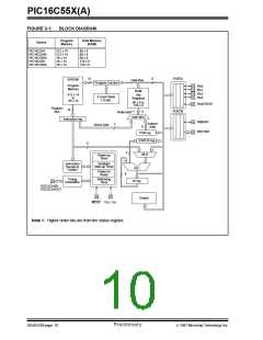
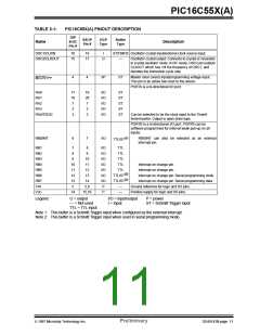
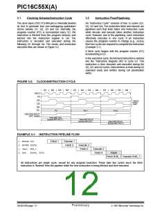
PIC16C55X(A)
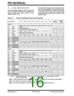
4.2.1
GENERAL PURPOSE REGISTER FILE
4.2
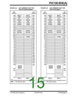
Data Memory Organization
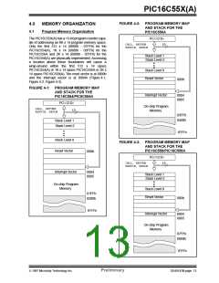
The register file is organized as 80 x 8 in the
PIC16C554(A)/556A and 128 x 8 in the PIC16C558(A).
Each is accessed either directly or indirectly through
the File Select Register, FSR (Section 4.4).
The data memory (Figure 4-4 and Figure 4-5) is
partitioned into two Banks which contain the general
purpose registers and the special function registers.
Bank 0 is selected when the RP0 bit is cleared. Bank 1
is selected when the RP0 bit (STATUS <5>) is set. The
Special Function Registers are located in the first 32
locations of each Bank. Register locations 20-6Fh
(Bank0) on the PIC16C554(A)/556A and 20-7Fh
(Bank0) and A0-BFh (Bank1) on the PIC16C558(A) are
general purpose registers implemented as static RAM.
Some special purpose registers are mapped in Bank 1.
DS40143B-page 14
Preliminary
1997 Microchip Technology Inc.

 MICROCHIP [ MICROCHIP ]