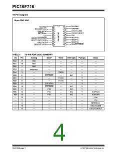
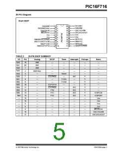
PIC16F716
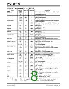
TABLE 1-1:
Name
PIC16F716 PINOUT DESCRIPTION
Function
Input Type Output Type
Description
Master clear (Reset) input. This pin is an active-low Reset to
the device.
MCLR/VPP
MCLR
ST
—
VPP
P
—
—
—
—
—
Programming voltage input
Oscillator crystal input
External clock source input
RC Oscillator mode
OSC1/CLKIN
OSC1
CLKIN
CLKIN
OSC2
XTAL
CMOS
ST
OSC2/CLKOUT
XTAL
Oscillator crystal output. Connects to crystal or resonator in
Crystal Oscillator mode.
CLKOUT
—
CMOS
In RC mode, OSC2 pin outputs CLKOUT which has 1/4 the
frequency of OSC1, and denotes the instruction cycle rate.
RA0/AN0
RA0
AN0
TTL
AN
TTL
AN
TTL
AN
TTL
AN
AN
ST
CMOS
—
Bidirectional I/O
Analog Channel 0 input
RA1/AN1
RA1
CMOS
—
Bidirectional I/O
AN1
Analog Channel 1 input
RA2/AN2
RA2
CMOS
—
Bidirectional I/O
AN2
Analog Channel 2 input
RA3/AN3/VREF
RA3
CMOS
—
Bidirectional I/O
AN3
Analog Channel 3 input
VREF
RA4
—
A/D reference voltage input
Bidirectional I/O. Open drain when configured as output.
Timer0 external clock input
Bidirectional I/O. Programmable weak pull-up.
External Interrupt
RA4/T0CKI
OD
T0CKI
RB0
ST
—
RB0/INT/ECCPAS2
TTL
ST
CMOS
—
INT
ECCPAS2
RB1
ST
—
ECCP Auto-Shutdown pin
Bidirectional I/O. Programmable weak pull-up.
RB1/T1OSO/T1CKI
TTL
—
CMOS
XTAL
T1OSO
Timer1 oscillator output. Connects to crystal in Oscillator
mode.
T1CKI
RB2
ST
TTL
XTAL
TTL
ST
—
Timer1 external clock input
RB2/T1OSI
CMOS
—
Bidirectional I/O. Programmable weak pull-up.
Timer1 oscillator input. Connects to crystal in Oscillator mode.
Bidirectional I/O. Programmable weak pull-up.
Capture1 input, Compare1 output, PWM1 output.
PWM P1A output
T1OSI
RB3
RB3/CCP1/P1A
CMOS
CMOS
CMOS
CMOS
CCP1
P1A
—
RB4/ECCPAS0
RB5/P1B
RB4
TTL
Bidirectional I/O. Programmable weak pull-up. Interrupt-on-
change.
ECCPAS0
RB5
ST
—
ECCP Auto-Shutdown pin
TTL
CMOS
Bidirectional I/O. Programmable weak pull-up. Interrupt-on-
change.
P1B
RB6
—
CMOS
CMOS
PWM P1B output
RB6/P1C
TTL
Bidirectional I/O. Programmable weak pull-up. Interrupt-on-
change. ST input when used as ICSP programming clock.
P1C
RB7
—
CMOS
CMOS
PWM P1C output
RB7/P1D
TTL
Bidirectional I/O. Programmable weak pull-up. Interrupt-on-
change. ST input when used as ICSP programming data.
P1D
VSS
VDD
AN
—
P
CMOS
—
PWM P1D output
VSS
VDD
Ground reference for logic and I/O pins.
Positive supply for logic and I/O pins.
P
—
Legend:
I
= Input
O = Output
= Power
= Analog input or output
OD
ST
= Open drain
= Schmitt Trigger input with CMOS levels
TTL = TTL compatible input
XTAL = Crystal
P
CMOS = CMOS compatible input or output
DS41206B-page 6
© 2007 Microchip Technology Inc.

 MICROCHIP [ MICROCHIP ]