PIC16F716
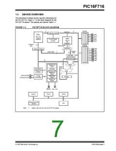
1.0
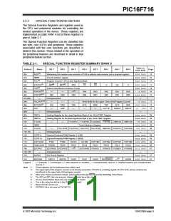
DEVICE OVERVIEW
This document contains device specific information for
the PIC16F716. Figure 1-1 is the block diagram for the
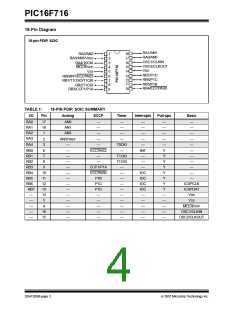
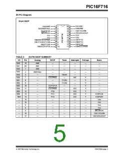
PIC16F716 device. The pinouts are listed in Table 1-1.
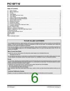
FIGURE 1-1:
PIC16F716 BLOCK DIAGRAM
13
8
PORTA
Data Bus
RAM
Program Counter
Flash
RA0
RA11
RA2
RA3
RA4
2K x 14
Program
Memory
8 Level Stack
(13-bit)
128 x 8
File
Registers
Program
Bus
14
RAM Addr(1)
PORTB
9
Addr MUX
RB0
RB1
RB2
RB3
RB4
RB5
RB6
RB7
Instruction Reg
Indirect
Addr
7
Direct Addr
8
FSR Reg
STATUS Reg
8
3
MUX
Power-up
Timer
Oscillator
Instruction
Decode and
Control
Start-up Timer
ALU
Power-on
Reset
8
OSC1/CLKIN
Timing
Generation
Watchdog
Timer
W Reg
OSC2/CLKOUT
Brown-out
Reset
MCLR VDD, VSS
Timer1
Timer2
A/D
Timer0
Enhanced CCP
(ECCP)
Note 1:
Higher order bits are from the STATUS register.
© 2007 Microchip Technology Inc.
DS41206B-page 5

 MICROCHIP [ MICROCHIP ]