PIC16F716
7.2.5
SPECIAL EVENT TRIGGER
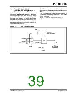
7.2
ADC Operation
The ECCP Special Event Trigger allows periodic ADC
measurements without software intervention. When
this trigger occurs, the GO/DONE bit is set by hardware
and the Timer1 counter resets to zero.
7.2.1
STARTING A CONVERSION
To enable the ADC module, the ADON bit of the
ADCON0 register must be set to a ‘1’. Setting the GO/
DONE bit of the ADCON0 register to a ‘1’ will start the
Analog-to-Digital conversion.
Using the Special Event Trigger does not assure proper
ADC timing. It is the user’s responsibility to ensure that
the ADC timing requirements are met.
Note:
The GO/DONE bit should not be set in the
same instruction that turns on the ADC.
Refer to Section 7.2.6 “A/D Conversion
Procedure”.
See Section 8.0 “Enhanced Capture/Compare/
PWM Module” for more information.
7.2.6
A/D CONVERSION PROCEDURE
7.2.2
COMPLETION OF A CONVERSION
This is an example procedure for using the ADC to
perform an Analog-to-Digital conversion:
When the conversion is complete, the ADC module will:
• Clear the GO/DONE bit
• Set the ADIF flag bit
1. Configure Port:
• Disable pin output driver (See TRIS register)
• Configure pin as analog
• Update the ADRES register with new conversion
result
2. Configure the ADC module:
• Select ADC conversion clock
• Configure voltage reference
• Select ADC input channel
• Select result format
7.2.3
TERMINATING A CONVERSION
If a conversion must be terminated before completion,
the GO/DONE bit can be cleared in software. The
ADRES register will not be updated with the partially
complete Analog-to-Digital conversion sample.
Instead, the ADRES register will retain the value of the
previous conversion. Additionally, a 2 TAD delay is
required before another acquisition can be initiated.
Following this delay, an input acquisition is automati-
cally started on the selected channel.
• Turn on ADC module
3. Configure ADC interrupt (optional):
• Clear ADC interrupt flag
• Enable ADC interrupt
• Enable peripheral interrupt
• Enable global interrupt(1)
4. Wait the required acquisition time(2)
Note:
A device Reset forces all registers to their
Reset state. Thus, the ADC module is
turned off and any pending conversion is
terminated.
.
5. Start conversion by setting the GO/DONE bit.
6. Wait for ADC conversion to complete by one of
the following:
7.2.4
ADC OPERATION DURING SLEEP
• Polling the GO/DONE bit
• Waiting for the ADC interrupt (interrupts
enabled)
The ADC module can operate during Sleep. This
requires the ADC clock source to be set to the FRC
option. When the FRC clock source is selected, the
ADC waits one additional instruction before starting the
conversion. This allows the SLEEP instruction to be
executed, which can reduce system noise during the
conversion. If the ADC interrupt is enabled, the device
will wake-up from Sleep when the conversion
completes. If the ADC interrupt is disabled, the ADC
module is turned off after the conversion completes,
although the ADON bit remains set.
7. Read ADC Result
8. Clear the ADC interrupt flag (required if interrupt
is enabled).
Note 1: The global interrupt can be disabled if the
user is attempting to wake-up from Sleep
and resume in-line code execution.
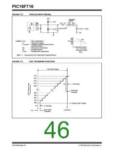
2: See Section 7.3 “A/D Acquisition
Requirements”.
When the ADC clock source is something other than
FRC, a SLEEP instruction causes the present conver-
sion to be aborted and the ADC module is turned off,
although the ADON bit remains set.
DS41206B-page 40
© 2007 Microchip Technology Inc.

 MICROCHIP [ MICROCHIP ]