PIC16F716
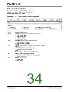
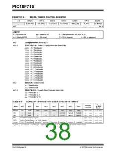
REGISTER 6-1:
T2CON: TIMER 2 CONTROL REGISTER
U-0
—
R/W-0
R/W-0
R/W-0
R/W-0
R/W-0
R/W-0
R/W-0
TOUTPS3
TOUTPS2
TOUTPS1
TOUTPS0
TMR2ON
T2CKPS1
T2CKPS0
bit 7
bit 0
Legend:
R = Readable bit
W = Writable bit
‘1’ = Bit is set
U = Unimplemented bit, read as ‘0’
‘0’ = Bit is cleared x = Bit is unknown
-n = Value at POR
bit 7
Unimplemented: Read as ‘0’
bit 6-3
TOUTPS<3:0>: Timer2 Output Postscaler Select bits
0000= 1:1 Postscaler
0001= 1:2 Postscaler
0010= 1:3 Postscaler
0011= 1:4 Postscaler
0100= 1:5 Postscaler
0101= 1:6 Postscaler
0110= 1:7 Postscaler
0111= 1:8 Postscaler
1000= 1:9 Postscaler
1001= 1:10 Postscaler
1010= 1:11 Postscaler
1011= 1:12 Postscaler
1100= 1:13 Postscaler
1101= 1:14 Postscaler
1110= 1:15 Postscaler
1111= 1:16 Postscaler
bit 2
TMR2ON: Timer2 On bit
1= Timer2 is on
0= Timer2 is off
bit 1-0
T2CKPS<1:0>: Timer2 Clock Prescale Select bits
00= Prescaler is 1
01= Prescaler is 4
1x= Prescaler is 16
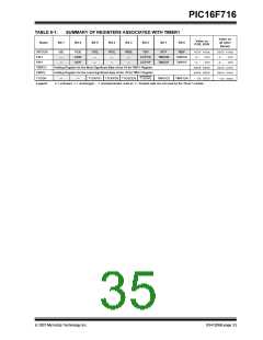
TABLE 6-1:
SUMMARY OF REGISTERS ASSOCIATED WITH TIMER2
Value on
all other
Resets
Value on
POR, BOR
Name
Bit 7
Bit 6
Bit 5
Bit 4
Bit 3
Bit 2
Bit 1
Bit 0
INTCON
PIE1
GIE
—
PEIE
ADIE
ADIF
T0IE
—
INTE
—
RBIE
—
T0IF
INTF
RBIF
0000 000x
-0-- -000
-0-- -000
1111 1111
0000 0000
-000 0000
0000 000x
-0-- -000
-0-- -000
1111 1111
0000 0000
-000 0000
CCP1IE
CCP1IF
TMR2IE
TMR2IF
TMR1IE
TMR1IF
PIR1
—
—
—
—
PR2
Timer2 Module Period Register
Holding Register for the 8-bit TMR2 Register
TOUTPS3 TOUTPS2 TOUTPS1 TOUTPS0
TMR2
T2CON
Legend:
—
TMR2ON
T2CKPS1
T2CKPS0
x= unknown, u= unchanged, -= unimplemented read as ‘0’. Shaded cells are not used for Timer2 module.
DS41206B-page 36
© 2007 Microchip Technology Inc.

 MICROCHIP [ MICROCHIP ]