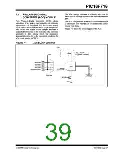
PIC16F716
7.2.7
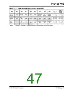
ADC REGISTER DEFINITIONS
The following registers are used to control the
operation of the ADC.
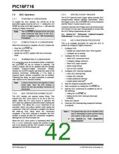
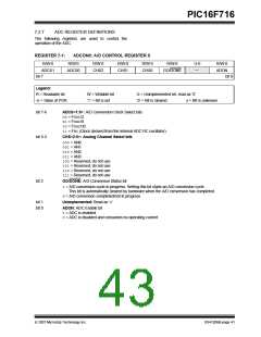
REGISTER 7-1:
ADCON0: A/D CONTROL REGISTER 0
R/W-0
R/W-0
R/W-0
CHS2
R/W-0
CHS1
R/W-0
CHS0
R/W-0
U-0
—
R/W-0
ADON
ADCS1
bit 7
ADCS0
GO/DONE
bit 0
Legend:
R = Readable bit
-n = Value at POR
W = Writable bit
‘1’ = Bit is set
U = Unimplemented bit, read as ‘0’
‘0’ = Bit is cleared x = Bit is unknown
bit 7-6
bit 5-3
ADCS<1:0>: A/D Conversion Clock Select bits
00= FOSC/2
01= FOSC/8
10= FOSC/32
11= FRC (Clock derived from the internal ADC RC oscillator)
CHS<2:0>: Analog Channel Select bits
000= AN0
001= AN1
010= AN2
011= AN3
100= Reserved, do not use
101= Reserved, do not use
110= Reserved, do not use
111= Reserved, do not use
bit 2
GO/DONE: A/D Conversion Status bit
1= A/D conversion cycle in progress. Setting this bit starts an A/D conversion cycle.
This bit is automatically cleared by hardware when the A/D conversion has completed.
0= A/D conversion completed/not in progress
bit 1
bit 0
Unimplemented: Read as ‘0’
ADON: ADC Enable bit
1= ADC is enabled
0= ADC is disabled and consumes no operating current
© 2007 Microchip Technology Inc.
DS41206B-page 41

 MICROCHIP [ MICROCHIP ]