PIC16F716
The ADC voltage reference is software selectable to
either VDD or a voltage applied to the external reference
pins.
7.0
ANALOG-TO-DIGITAL
CONVERTER (ADC) MODULE
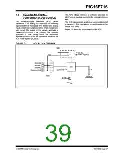
The Analog-to-Digital Converter (ADC) allows
conversion of an analog input signal to a 8-bit binary
representation of that signal. This device uses analog
inputs, which are multiplexed into a single sample and
hold circuit. The output of the sample and hold is
connected to the input of the converter. The converter
The ADC can generate an interrupt upon completion of
a conversion. This interrupt can be used to wake-up the
device from Sleep.
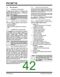
Figure 7-1 shows the block diagram of the ADC.
generates
a 8-bit binary result via successive
approximation and stores the conversion result into the
ADC result register (ADRES).
FIGURE 7-1:
ADC BLOCK DIAGRAM
VDD
PFCG<2:0>
(ADCON1 register)
VREF
000
001
010
011
RA0/AN0
RA1/AN1
ADC
RA2/AN2
8
GO/DONE
RA3/VREF/AN3
CHS
ADRES
ADON
VSS
© 2007 Microchip Technology Inc.
DS41206B-page 37

 MICROCHIP [ MICROCHIP ]