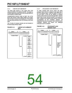
PIC16F/LF1946/47
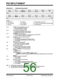
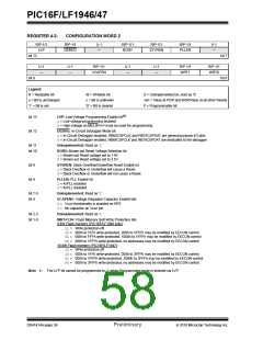
REGISTER 4-2:
CONFIGURATION WORD 2
R/P-1/1
LVP
R/P-1/1
DEBUG
U-1
—
R/P-1/1
BORV
R/P-1/1
R/P-1/1
PLLEN
U-1
—
STVREN
bit 13
bit 7
bit 0
U-1
—
U-1
—
R/P-1/1
U-1
—
U-1
—
R/P-1/1
WRT1
R/P-1/1
WRT0
VCAPEN
bit 6
Legend:
R = Readable bit
u = Bit is unchanged
‘1’ = Bit is set
W = Writable bit
x = Bit is unknown
‘0’ = Bit is cleared
U = Unimplemented bit, read as ‘0’
-n/n = Value at POR and BOR/Value at all other Resets
P = Programmable bit
(1)
bit 13
bit 12
LVP: Low-Voltage Programming Enable bit
1= Low-voltage programming enabled
0= High-voltage on MCLR/VPP must be used for programming
DEBUG: In-Circuit Debugger Mode bit
1= In-Circuit Debugger disabled, RB6/ICSPCLK and RB7/ICSPDAT are general purpose I/O pins
0= In-Circuit Debugger enabled, RB6/ICSPCLK and RB7/ICSPDAT are dedicated to the debugger
bit 11
bit 10
Unimplemented: Read as ‘1’
BORV: Brown-out Reset Voltage Selection bit
1= Brown-out Reset voltage set to 1.9V
0= Brown-out Reset voltage set to 2.5V
bit 9
bit 8
STVREN: Stack Overflow/Underflow Reset Enable bit
1= Stack Overflow or Underflow will cause a Reset
0= Stack Overflow or Underflow will not cause a Reset
PLLEN: PLL Enable bit
1= 4xPLL enabled
0= 4xPLL disabled
bit 7-5
bit 4
Unimplemented: Read as ‘1’
VCAPEN>: Voltage Regulator Capacitor Enable bits
0= VCAP functionality is enabled on RF0
1= No capacitor on VCAP pin
bit 2-3
bit 1-0
Unimplemented: Read as ‘1’
WRT<1:0>: Flash Memory Self-Write Protection bits
8 kW Flash memory (PIC16F/LF1946 only):
11= Write protection off
10= 000h to 1FFh write-protected, 200h to 1FFFh may be modified by EECON control
01= 000h to FFFh write-protected, 1000h to 1FFFh may be modified by EECON control
00= 000h to 1FFFh write-protected, no addresses may be modified by EECON control
16 kW Flash memory (PIC16F/LF1947):
11= Write protection off
10= 000h to 1FFh write-protected, 200h to 3FFFh may be modified by EECON control
01= 000h to 1FFFh write-protected, 2000h to 3FFFh may be modified by EECON control
00= 000h to 3FFFh write-protected, no addresses may be modified by EECON control
Note 1: The LVP bit cannot be programmed to ‘0’ when Programming mode is entered via LVP.
DS41414A-page 56
Preliminary
2010 Microchip Technology Inc.

 MICROCHIP [ MICROCHIP ]