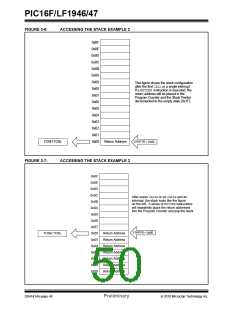
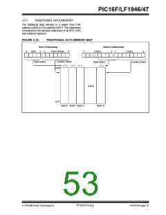
PIC16F/LF1946/47
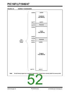
3.5.2
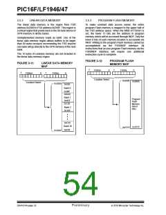
LINEAR DATA MEMORY
3.5.3
PROGRAM FLASH MEMORY
The linear data memory is the region from FSR
address 0x2000 to FSR address 0x29AF. This region is
a virtual region that points back to the 80-byte blocks of
GPR memory in all the banks.
To make constant data access easier, the entire
program Flash memory is mapped to the upper half of
the FSR address space. When the MSB of FSRnH is
set, the lower 15 bits are the address in program
memory which will be accessed through INDF. Only the
lower 8 bits of each memory location is accessible via
INDF. Writing to the program Flash memory cannot be
accomplished via the FSR/INDF interface. All
instructions that access program Flash memory via the
FSR/INDF interface will require one additional
instruction cycle to complete.
Unimplemented memory reads as 0x00. Use of the
linear data memory region allows buffers to be larger
than 80 bytes because incrementing the FSR beyond
one bank will go directly to the GPR memory of the next
bank.
The 16 bytes of common memory are not included in
the linear data memory region.
FIGURE 3-12:
PROGRAM FLASH
MEMORY MAP
FIGURE 3-11:
LINEAR DATA MEMORY
MAP
7
7
0
0
FSRnH
FSRnL
7
1
7
0
0
FSRnH
FSRnL
0
0 1
Location Select
0x8000
0x0000
Location Select
0x2000
0x020
Bank 0
0x06F
0x0A0
Bank 1
0x0EF
0x120
Program
Flash
Memory
(low 8
bits)
Bank 2
0x16F
0xF20
Bank 30
0x7FFF
0xFFFF
0xF6F
0x29AF
DS41414A-page 52
Preliminary
2010 Microchip Technology Inc.

 MICROCHIP [ MICROCHIP ]