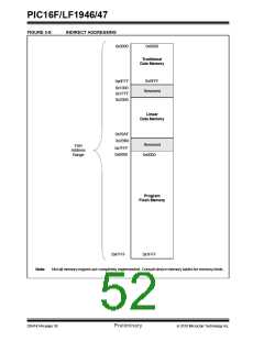
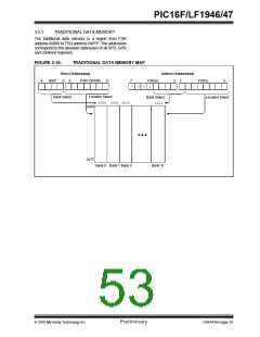
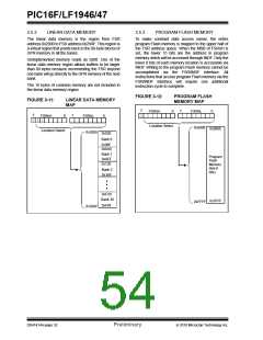
PIC16F/LF1946/47
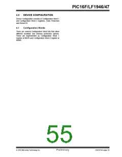
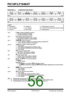
REGISTER 4-1:
CONFIGURATION WORD 1
R/P-1/1
FCMEN
bit 13
R/P-1/1
IESO
R/P-1/1
R/P-1/1
R/P-1/1
R/P-1/1
CPD
R/P-1/1
CP
CLKOUTEN
BOREN1
BOREN0
bit 7
bit 0
R/P-1/1
MCLRE
bit 6
R/P-1/1
PWRTE
R/P-1/1
WDTE1
R/P-1/1
WDTE0
R/P-1/1
FOSC2
R/P-1/1
FOSC1
R/P-1/1
FOSC0
Legend:
R = Readable bit
u = Bit is unchanged
‘1’ = Bit is set
W = Writable bit
x = Bit is unknown
‘0’ = Bit is cleared
U = Unimplemented bit, read as ‘0’
-n/n = Value at POR and BOR/Value at all other Resets
P = Programmable bit
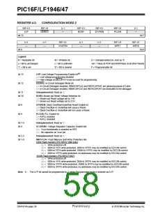
bit 13
bit 12
bit 11
FCMEN: Fail-Safe Clock Monitor Enable bit
1= Fail-Safe Clock Monitor is enabled
0= Fail-Safe Clock Monitor is disabled
IESO: Internal External Switchover bit
1= Internal/External Switchover mode is enabled
0= Internal/External Switchover mode is disabled
CLKOUTEN: Clock Out Enable bit
1= CLKOUT function is disabled. I/O or oscillator function on RA6/CLKOUT
0= CLKOUT function is enabled on RA6/CLKOUT
(1)
bit 10-9
BOREN<1:0>: Brown-out Reset Enable bits
11= BOR enabled
10= BOR enabled during operation and disabled in Sleep
01= BOR controlled by SBOREN bit of the BORCON register
00= BOR disabled
(2)
bit 8
bit 7
bit 6
CPD: Data Code Protection bit
1= Data memory code protection is disabled
0= Data memory code protection is enabled
(3)
CP: Code Protection bit
1= Program memory code protection is disabled
0= Program memory code protection is enabled
MCLRE: RE3/MCLR/VPP Pin Function Select bit
If LVP bit = 1:
This bit is ignored.
If LVP bit = 0:
1= RE3/MCLR/VPP pin function is MCLR; Weak pull-up enabled.
0= RE3/MCLR/VPP pin function is digital input; MCLR internally disabled; Weak pull-up under control of WPUE3
bit.
(1)
bit 5
PWRTE: Power-up Timer Enable bit
1= PWRT disabled
0= PWRT enabled
bit 4-3
WDTE<1:0>: Watchdog Timer Enable bit
11= WDT enabled
10= WDT enabled while running and disabled in Sleep
01= WDT controlled by the SWDTEN bit in the WDTCON register
00= WDT disabled
Note 1: Enabling Brown-out Reset does not automatically enable Power-up Timer.
2: The entire data EEPROM will be erased when the code protection is turned off during an erase.
3: The entire program memory will be erased when the code protection is turned off.
DS41414A-page 54
Preliminary
2010 Microchip Technology Inc.

 MICROCHIP [ MICROCHIP ]