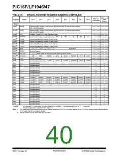
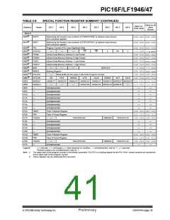
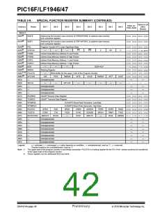
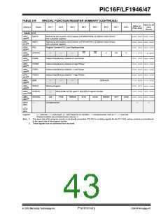
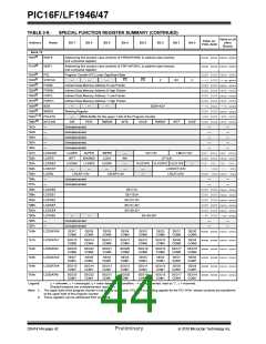
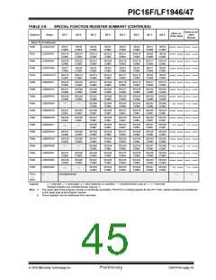
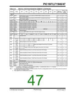
PIC16F/LF1946/47
TABLE 3-9:
SPECIAL FUNCTION REGISTER SUMMARY (CONTINUED)
Value on all
other
Resets
Value on:
POR, BOR
Address
Name
Bit 7
Bit 6
Bit 5
Bit 4
Bit 3
Bit 2
Bit 1
Bit 0
Bank 15
780h(2)
INDF0
INDF1
Addressing this location uses contents of FSR0H/FSR0L to address data memory
(not a physical register)
xxxx xxxx xxxx xxxx
xxxx xxxx xxxx xxxx
781h(2)
Addressing this location uses contents of FSR1H/FSR1L to address data memory
(not a physical register)
782h(2)
783h(2)
784h(2)
785h(2)
786h(2)
787h(2)
788h(2)
789h(2)
PCL
Program Counter (PC) Least Significant Byte
0000 0000 0000 0000
---1 1000 ---q quuu
0000 0000 uuuu uuuu
0000 0000 0000 0000
0000 0000 uuuu uuuu
0000 0000 0000 0000
---0 0000 ---0 0000
0000 0000 uuuu uuuu
-000 0000 -000 0000
0000 000x 0000 000u
STATUS
FSR0L
FSR0H
FSR1L
FSR1H
BSR
—
—
—
TO
PD
Z
DC
C
Indirect Data Memory Address 0 Low Pointer
Indirect Data Memory Address 0 High Pointer
Indirect Data Memory Address 1 Low Pointer
Indirect Data Memory Address 1 High Pointer
—
—
—
BSR<4:0>
WREG
Working Register
78Ah(1, 2) PCLATH
—
Write Buffer for the upper 7 bits of the Program Counter
78Bh(2)
78Ch
78Dh
78Eh
78Fh
790h
791h
792h
793h
794h
795h
796h
797h
798h
799h
79Ah
79Bh
79Ch
79Dh
79Eh
79Fh
7A0h
INTCON
—
GIE
PEIE
TMR0IE
INTE
IOCIE
TMR0IF
INTF
IOCIF
Unimplemented
Unimplemented
Unimplemented
Unimplemented
Unimplemented
—
—
—
—
—
—
—
—
—
—
—
—
—
—
LCDCON
LCDPS
LCDREF
LCDCST
LCDRL
—
LCDEN
WFT
SLPEN
WERR
LCDA
LCDIRI
—
—
WA
—
CS<1:0>
LMUX<1:0>
000- 0011 000- 0011
0000 0000 0000 0000
000- 000- 000- 000-
---- -000 ---- -000
0000 -000 0000 -000
BIASMD
LCDIRS
—
LP<3:0>
VLCD3PE VLCD2PE VLCD1PE
LCDIRE
—
—
—
—
—
LCDCST<2:0>
LRLAT<2:0>
LRLAP<1:0>
LRLBP<1:0>
Unimplemented
Unimplemented
—
—
—
—
—
LCDSE0
LCDSE1
LCDSE2
LCDSE3
LCDSE4
LCDSE5
—
SE<7:0>
0000 0000 uuuu uuuu
0000 0000 uuuu uuuu
0000 0000 uuuu uuuu
0000 0000 uuuu uuuu
0000 0000 uuuu uuuu
--00 0000 --uu uuuu
SE<15:8>
SE<23:16>
SE<31:24>
SE<39:32>
—
—
SE<45:40>
Unimplemented
Unimplemented
—
—
—
—
—
LCDDATA0
SEG7
COM0
SEG6
COM0
SEG5
COM0
SEG4
COM0
SEG3
COM0
SEG2
COM0
SEG1
COM0
SEG0
COM0
xxxx xxxx uuuu uuuu
7A1h
LCDDATA1
LCDDATA2
LCDDATA3
LCDDATA4
LCDDATA5
SEG15
COM0
SEG14
COM0
SEG13
COM0
SEG12
COM0
SEG11
COM0
SEG10
COM0
SEG9
COM0
SEG8
COM0
xxxx xxxx uuuu uuuu
7A2h
SEG23
COM0
SEG22
COM0
SEG21
COM0
SEG20
COM0
SEG19
COM0
SEG18
COM0
SEG17
COM0
SEG16 xxxx xxxx uuuu uuuu
COM0
7A3h
SEG7
COM1
SEG6
COM1
SEG5
COM1
SEG4
COM1
SEG3
COM1
SEG2
COM1
SEG1
COM1
SEG0
COM1
xxxx xxxx uuuu uuuu
xxxx xxxx uuuu uuuu
7A4h
SEG15
COM1
SEG14
COM1
SEG13
COM1
SEG12
COM1
SEG11
COM1
SEG10
COM1
SEG9
COM1
SEG8
COM1
7A5h
SEG23
COM1
SEG22
COM1
SEG21
COM1
SEG20
COM1
SEG19
COM1
SEG18
COM1
SEG17
COM1
SEG16 xxxx xxxx uuuu uuuu
COM1
Legend:
x= unknown, u= unchanged, q= value depends on condition, - = unimplemented, read as ‘0’, r= reserved.
Shaded locations are unimplemented, read as ‘0’.
Note 1: The upper byte of the program counter is not directly accessible. PCLATH is a holding register for the PC<14:8>, whose contents are transferred
to the upper byte of the program counter.
2: These registers can be addressed from any bank.
DS41414A-page 42
Preliminary
2010 Microchip Technology Inc.

 MICROCHIP [ MICROCHIP ]