PIC16F/LF1946/47
TABLE 29-10: COMPARATOR SPECIFICATIONS
Operating Conditions: 1.8V < VDD < 5.5V, -40°C < TA < +125°C (unless otherwise stated).
Param
No.
Sym.
Characteristics
Input Offset Voltage
Min.
Typ.
Max.
Units
Comments
CM01
VIOFF
—
0
±7.5
—
±60
VDD
—
mV
V
CM02
CM03
CM04
CM05
VICM
Input Common Mode Voltage
Common Mode Rejection Ratio
Response Time
CMRR
TRESP
—
—
—
50
dB
ns
s
150
—
400
10
Note 1
TMC2OV Comparator Mode Change to
Output Valid*
CM06
CHYSTER Comparator Hysteresis
—
65
—
mV
*
These parameters are characterized but not tested.
Note 1: Response time measured with one comparator input at VDD/2, while the other input transitions
from VSS to VDD.
TABLE 29-11: DIGITAL-TO-ANALOG CONVERTER (DAC) SPECIFICATIONS
Operating Conditions: 1.8V < VDD < 5.5V, -40°C < TA < +125°C (unless otherwise stated).
Param
No.
Sym.
Characteristics
Step Size(2)
Min.
Typ.
Max.
Units
Comments
DAC01*
DAC02*
DAC03*
DAC04*
*
CLSB
—
—
—
—
VDD/32
—
—
1/2
—
V
LSb
CACC
CR
Absolute Accuracy
Unit Resistor Value (R)
Settling Time(1)
TBD
—
CST
10
s
These parameters are characterized but not tested.
Legend: TBD = To Be Determined
Note 1: Settling time measured while DACR<4:0> transitions from ‘0000’ to ‘1111’.
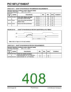
FIGURE 29-14:
USART SYNCHRONOUS TRANSMISSION (MASTER/SLAVE) TIMING
CK
DT
US121
US121
US122
US120
Refer to Figure 29-5 for load conditions.
Note:
2010 Microchip Technology Inc.
Preliminary
DS41414A-page 405

 MICROCHIP [ MICROCHIP ]