PIC16F/LF1946/47
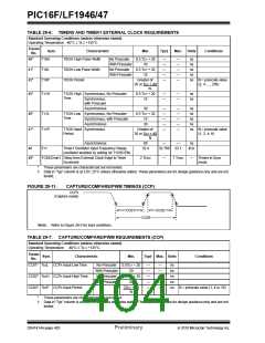
TABLE 29-8: PIC16F/LF1946/47 A/D CONVERTER (ADC) CHARACTERISTICS:
Standard Operating Conditions (unless otherwise stated)
Operating temperature -40°C TA +125°C
Param
No.
Sym.
Characteristic
Min.
Typ†
Max. Units
Conditions
AD01 NR
AD02 EIL
AD03 EDL
Resolution
—
—
—
—
—
—
10
±1.7
±1
bit
Integral Error
LSb VREF = 3.0V
Differential Error
LSb No missing codes
VREF = 3.0V
AD04 EOFF Offset Error
—
—
—
—
—
—
—
±2
±1.5
VDD
VREF
50
LSb VREF = 3.0V
AD05 EGN Gain Error
LSb VREF = 3.0V
(3)
AD06 VREF Reference Voltage
AD07 VAIN Full-Scale Range
1.8
VSS
—
V
V
AD08 ZAIN Recommended Impedance of
Analog Voltage Source
k Can go higher if external 0.01F capacitor is
present on input pin.
*
These parameters are characterized but not tested.
†
Data in “Typ” column is at 3.0V, 25°C unless otherwise stated. These parameters are for design guidance only and are not
tested.
Note 1: Total Absolute Error includes integral, differential, offset and gain errors.
2: The A/D conversion result never decreases with an increase in the input voltage and has no missing codes.
3: ADC VREF is from external VREF, VDD pin or FVREF, whichever is selected as reference input.
4: When ADC is off, it will not consume any current other than leakage current. The power-down current specification
includes any such leakage from the ADC module.
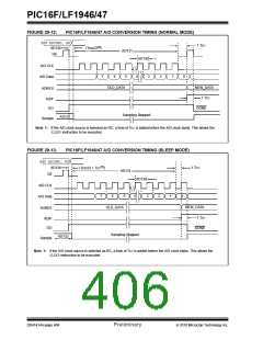
TABLE 29-9: PIC16F/LF1946/47 A/D CONVERSION REQUIREMENTS
Standard Operating Conditions (unless otherwise stated)
Operating temperature
-40°C TA +125°C
Param
Sym.
No.
Characteristic
Min.
Typ†
Max. Units
Conditions
AD130* TAD
A/D Clock Period
1.0
1.0
—
9.0
6.0
s
s
TOSC-based
ADCS<1:0> = 11(ADRC mode)
A/D Internal RC Oscillator
Period
1.6
AD131 TCNV Conversion Time (not including
—
—
11
—
—
TAD Set GO/DONE bit to conversion
complete
(1)
Acquisition Time)
AD132* TACQ Acquisition Time
5.0
s
*
These parameters are characterized but not tested.
†
Data in “Typ” column is at 3.0V, 25°C unless otherwise stated. These parameters are for design guidance only and are not
tested.
Note 1: The ADRES register may be read on the following TCY cycle.
2010 Microchip Technology Inc.
Preliminary
DS41414A-page 403

 MICROCHIP [ MICROCHIP ]