PIC16F/LF1946/47
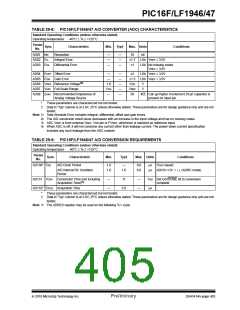
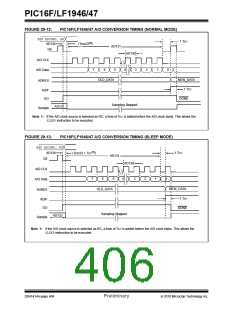
FIGURE 29-12:
PIC16F/LF1946/47 A/D CONVERSION TIMING (NORMAL MODE)
BSF ADCON0, GO
1 TCY
(1)
(TOSC/2
AD134
Q4
)
AD131
AD130
A/D CLK
7
6
5
4
3
2
1
0
A/D Data
ADRES
NEW_DATA
1 TCY
OLD_DATA
ADIF
GO
DONE
Sampling Stopped
AD132
Sample
Note 1: If the A/D clock source is selected as RC, a time of TCY is added before the A/D clock starts. This allows the
SLEEPinstruction to be executed.
FIGURE 29-13:
PIC16F/LF1946/47 A/D CONVERSION TIMING (SLEEP MODE)
BSF ADCON0, GO
AD134
Q4
(1)
(TOSC/2 + TCY
1 TCY
)
AD131
AD130
A/D CLK
A/D Data
7
6
5
3
2
1
0
4
NEW_DATA
1 TCY
OLD_DATA
ADRES
ADIF
GO
DONE
Sampling Stopped
AD132
Sample
Note 1: If the A/D clock source is selected as RC, a time of TCY is added before the A/D clock starts. This allows the
SLEEPinstruction to be executed.
DS41414A-page 404
Preliminary
2010 Microchip Technology Inc.

 MICROCHIP [ MICROCHIP ]