PIC16F/LF1946/47
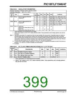
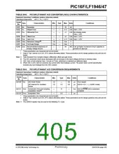
TABLE 29-4: CLKOUT AND I/O TIMING PARAMETERS
Standard Operating Conditions (unless otherwise stated)
Operating Temperature -40°C TA +125°C
Param
No.
Sym.
Characteristic
Min.
Typ† Max. Units
Conditions
OS11 TosH2ckL FOSC to CLKOUT (1)
OS12 TosH2ckH FOSC to CLKOUT (1)
OS13 TckL2ioV CLKOUT to Port out valid(1)
—
—
—
—
—
—
70
72
20
ns VDD = 3.3-5.0V
ns VDD = 3.3-5.0V
ns
OS14 TioV2ckH Port input valid before CLKOUT(1)
OS15 TosH2ioV Fosc (Q1 cycle) to Port out valid
TOSC + 200 ns
—
50
—
—
70*
—
ns
—
ns VDD = 3.3-5.0V
ns VDD = 3.3-5.0V
OS16 TosH2ioI
Fosc (Q2 cycle) to Port input invalid
50
(I/O in hold time)
OS17 TioV2osH Port input valid to Fosc(Q2 cycle)
20
—
—
ns
(I/O in setup time)
OS18 TioR
OS19 TioF
Port output rise time(2)
—
—
40
15
72
32
ns
ns
VDD = 1.8V
VDD = 3.3-5.0V
Port output fall time(2)
—
—
28
15
55
30
VDD = 1.8V
VDD = 3.3-5.0V
OS20* Tinp
OS21* Tioc
INT pin input high or low time
25
25
—
—
—
—
ns
ns
Interrupt-on-change new input level
time
*
†
These parameters are characterized but not tested.
Data in “Typ” column is at 3.0V, 25C unless otherwise stated.
Note 1: Measurements are taken in RC mode where CLKOUT output is 4 x TOSC.
2: Includes OSC2 in CLKOUT mode.
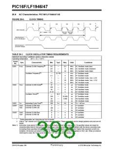
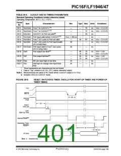
FIGURE 29-8:
RESET, WATCHDOG TIMER, OSCILLATOR START-UP TIMER AND POWER-UP
TIMER TIMING
VDD
MCLR
30
Internal
POR
33
PWRT
Time-out
32
OSC
Start-Up Time
(1)
Internal Reset
Watchdog Timer
(1)
Reset
31
34
34
I/O pins
Note 1: Asserted low.
2010 Microchip Technology Inc.
Preliminary
DS41414A-page 399

 MICROCHIP [ MICROCHIP ]