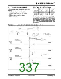
PIC16F/LF1946/47
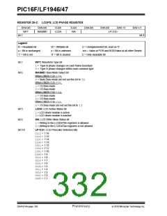
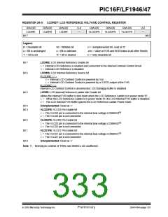
REGISTER 26-3: LCDREF: LCD REFERENCE VOLTAGE CONTROL REGISTER
R/W-0/0
LCDIRE
R/W-0/0
LCDIRS
R/W-0/0
LCDIRI
U-0
—
R/W-0/0
R/W-0/0
R/W-0/0
U-0
—
VLCD3PE
VLCD2PE
VLCD1PE
bit 7
bit 0
Legend:
R = Readable bit
W = Writable bit
x = Bit is unknown
‘0’ = Bit is cleared
U = Unimplemented bit, read as ‘0’
u = Bit is unchanged
‘1’ = Bit is set
-n/n = Value at POR and BOR/Value at all other Resets
C = Only clearable bit
bit 7
bit 6
LCDIRE: LCD Internal Reference Enable bit
1= Internal LCD Reference is enabled and connected to the Internal Contrast Control circuit
0= Internal LCD Reference is disabled
LCDIRS: LCD Internal Reference Source bit
If LCDIRE = 1:
0= Internal LCD Contrast Control is powered by VDD
1= Internal LCD Contrast Control is powered by a 3.072V output of the FVR.
If LCDIRE = 0:
Internal LCD Contrast Control is unconnected. LCD bandgap buffer is disabled.
bit 5
LCDIRI: LCD Internal Reference Ladder Idle Enable bit
Allows the Internal FVR buffer to shut down when the LCD Reference Ladder is in power mode ‘B’
1= When the LCD Reference Ladder is in power mode ‘B’, the LCD Internal FVR buffer is disabled.
0= The LCD Internal FVR Buffer ignores the LCD Reference Ladder Power mode.
bit 4
bit 3
Unimplemented: Read as ‘0’
VLCD3PE: VLCD3 Pin Enable bit
1= The VLCD3 pin is connected to the internal bias voltage LCDBIAS3(1)
0= The VLCD3 pin is not connected
bit 2
bit 1
bit 0
VLCD2PE: VLCD2 Pin Enable bit
1= The VLCD2 pin is connected to the internal bias voltage LCDBIAS2(1)
0= The VLCD2 pin is not connected
VLCD1PE: VLCD1 Pin Enable bit
1= The VLCD1 pin is connected to the internal bias voltage LCDBIAS1(1)
0= The VLCD1 pin is not connected
Unimplemented: Read as ‘0’
Note 1: Normal pin controls of TRISx and ANSELx are unaffected.
2010 Microchip Technology Inc.
Preliminary
DS41414A-page 331

 MICROCHIP [ MICROCHIP ]