PIC16F/LF1946/47
TABLE 26-2: LCD BIAS VOLTAGES
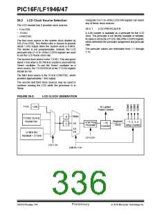
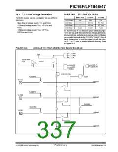
26.3 LCD Bias Voltage Generation
Static Bias
1/2 Bias
1/3 Bias
The LCD module can be configured for one of three
bias types:
LCD Bias 0
LCD Bias 1
LCD Bias 2
LCD Bias 3
VSS
—
VSS
VSS
1/2 VDD
1/2 VDD
VLCD3
1/3 VDD
2/3 VDD
VLCD3
• Static Bias (2 voltage levels: VSS and VLCD)
—
• 1/2 Bias (3 voltage levels: VSS, 1/2 VLCD and
VLCD)
VLCD3
• 1/3 Bias (4 voltage levels: VSS, 1/3 VLCD,
2/3 VLCD and VLCD)
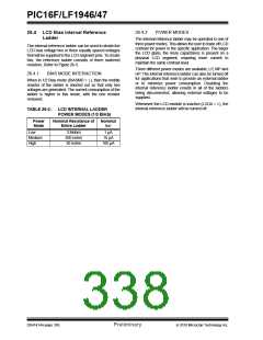
So that the user is not forced to place external compo-
nents and use up to three pins for bias voltage generation,
internal contrast control and an internal reference ladder
are provided internally to the PIC16F/LF1946/47. Both of
these features may be used in conjunction with the exter-
nal VLCD<3:1> pins, to provide maximum flexibility. Refer
to Figure 26-3.
FIGURE 26-3:
LCD BIAS VOLTAGE GENERATION BLOCK DIAGRAM
LCDIRE
LCDIRS
LCDA
VDD
1.024V from
FVR
3.072V
x 3
LCDRLP1
LCDRLP0
LCDIRE
LCDIRS
LCDA
LCDCST<2:0>
VLCD3PE
LCDA
VLCD3
lcdbias3
VLCD2PE
VLCD2
lcdbias2
BIASMD
VLCD1PE
VLCD1
lcdbias1
lcdbias0
2010 Microchip Technology Inc.
Preliminary
DS41414A-page 335

 MICROCHIP [ MICROCHIP ]