PIC16F/LF1946/47
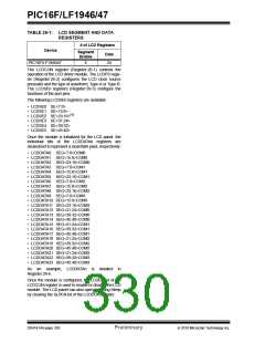
TABLE 26-1: LCD SEGMENT AND DATA
REGISTERS
# of LCD Registers
Device
Segment
Enable
Data
PIC16F/LF1946/47
6
24
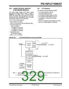
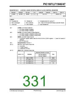
The LCDCON register (Register 26-1) controls the
operation of the LCD driver module. The LCDPS regis-
ter (Register 26-2) configures the LCD clock source
prescaler and the type of waveform; Type-A or Type-B.
The LCDSEn registers (Register 26-5) configure the
functions of the port pins.
The following LCDSEn registers are available:
• LCDSE0 SE<7:0>
• LCDSE1 SE<15:8>
• LCDSE2 SE<23:16>(1)
• LCDSE3 SE<31:24>
• LCDSE4 SE<39:32>
• LCDSE5 SE<45:40>
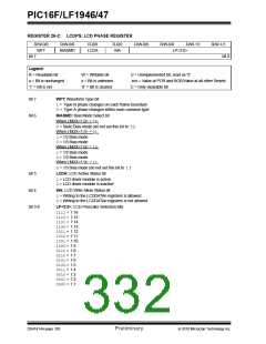
Once the module is initialized for the LCD panel, the
individual bits of the LCDDATAn registers are
cleared/set to represent a clear/dark pixel, respectively:
• LCDDATA0 SEG<7:0>COM0
• LCDDATA1 SEG<15:8>COM0
• LCDDATA2 SEG<23:16>COM0
• LCDDATA3 SEG<7:0>COM1
• LCDDATA4 SEG<15:8>COM1
• LCDDATA5 SEG<23:16>COM1
• LCDDATA6 SEG<7:0>COM2
• LCDDATA7 SEG<15:8>COM2
• LCDDATA8 SEG<23:16>COM2
• LCDDATA9 SEG<7:0>COM3
• LCDDATA10 SEG<15:8>COM3
• LCDDATA11 SEG<23:16>COM3
• LCDDATA12 SEG<31:24>COM0
• LCDDATA13 SEG<39:32>COM0
• LCDDATA14 SEG<45:40>COM0
• LCDDATA15 SEG<31:24>COM1
• LCDDATA16 SEG<39:32>COM1
• LCDDATA17 SEG<45:40>COM1
• LCDDATA18 SEG<31:24>COM2
• LCDDATA19 SEG<39:32>COM2
• LCDDATA20 SEG<45:40>COM2
• LCDDATA21 SEG<31:24>COM3
• LCDDATA22 SEG<39:32>COM3
• LCDDATA23 SEG<45:40>COM3
As an example, LCDDATAn is detailed in
Register 26-6.
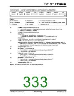
Once the module is configured, the LCDEN bit of the
LCDCON register is used to enable or disable the LCD
module. The LCD panel can also operate during Sleep
by clearing the SLPEN bit of the LCDCON register.
DS41414A-page 328
Preliminary
2010 Microchip Technology Inc.

 MICROCHIP [ MICROCHIP ]