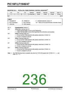
PIC16F/LF1946/47
its SDOx pin) and the slave device is reading this bit
and saving it as the LSb of its shift register, that the
slave device is also sending out the MSb from its shift
register (on its SDOx pin) and the master device is
reading this bit and saving it as the LSb of its shift
register.
23.2 SPI Mode Overview
The Serial Peripheral Interface (SPI) bus is a
synchronous serial data communication bus that
operates in Full Duplex mode. Devices communicate in
a master/slave environment where the master device
initiates the communication.
A slave device is
After 8 bits have been shifted out, the master and slave
have exchanged register values.
controlled through a chip select known as Slave Select.
The SPI bus specifies four signal connections:
If there is more data to exchange, the shift registers are
loaded with new data and the process repeats itself.
• Serial Clock (SCKx)
• Serial Data Out (SDOx)
• Serial Data In (SDIx)
• Slave Select (SSx)
Whether the data is meaningful or not (dummy data),
depends on the application software. This leads to
three scenarios for data transmission:
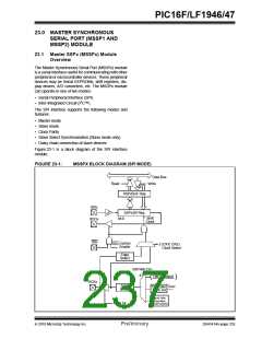
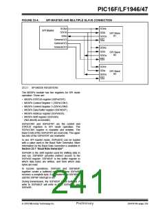
Figure 23-1 shows the block diagram of the MSSPx
module when operating in SPI Mode.
• Master sends useful data and slave sends dummy
data.
• Master sends useful data and slave sends useful
data.
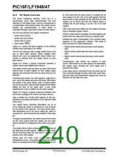
The SPI bus operates with a single master device and
one or more slave devices. When multiple slave
devices are used, an independent Slave Select con-
nection is required from the master device to each
slave device.
• Master sends dummy data and slave sends useful
data.
Transmissions may involve any number of clock
cycles. When there is no more data to be transmitted,
the master stops sending the clock signal and it
deselects the slave.
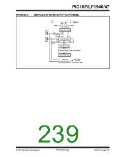
Figure 23-4 shows a typical connection between a
master device and multiple slave devices.
The master selects only one slave at a time. Most slave
devices have tri-state outputs so their output signal
appears disconnected from the bus when they are not
selected.
Every slave device connected to the bus that has not
been selected through its slave select line must disre-
gard the clock and transmission signals and must not
transmit out any data of its own.
Transmissions involve two shift registers, eight bits in
size, one in the master and one in the slave. With either
the master or the slave device, data is always shifted
out one bit at a time, with the Most Significant bit (MSb)
shifted out first. At the same time, a new Least
Significant bit (LSb) is shifted into the same register.
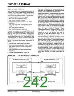
Figure 23-5 shows a typical connection between two
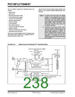
processors configured as master and slave devices.
Data is shifted out of both shift registers on the pro-
grammed clock edge and latched on the opposite edge
of the clock.
The master device transmits information out on its
SDOx output pin which is connected to, and received
by, the slave’s SDIx input pin. The slave device trans-
mits information out on its SDOx output pin, which is
connected to, and received by, the master’s SDIx input
pin.
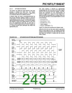
To begin communication, the master device first sends
out the clock signal. Both the master and the slave
devices should be configured for the same clock polar-
ity.
The master device starts a transmission by sending out
the MSb from its shift register. The slave device reads
this bit from that same line and saves it into the LSb
position of its shift register.
During each SPI clock cycle, a full duplex data
transmission occurs. This means that while the master
device is sending out the MSb from its shift register (on
DS41414A-page 238
Preliminary
2010 Microchip Technology Inc.

 MICROCHIP [ MICROCHIP ]