PIC16F/LF1946/47
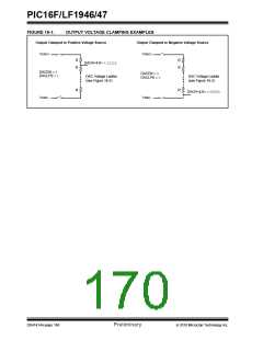
16.3.1
OUTPUT CLAMPED TO POSITIVE
VOLTAGE SOURCE
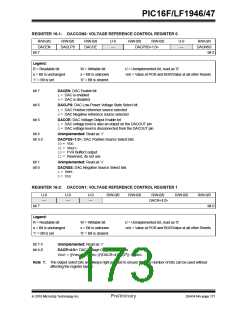
16.0 DIGITAL-TO-ANALOG
CONVERTER (DAC) MODULE
The DAC output voltage can be set to VSRC+ with the
least amount of power consumption by performing the
following:
The Digital-to-Analog Converter supplies a variable
voltage reference, ratiometric with the input source,
with 32 selectable output levels.
• Clearing the DACEN bit in the DACCON0 register.
• Setting the DACLPS bit in the DACCON0 register.
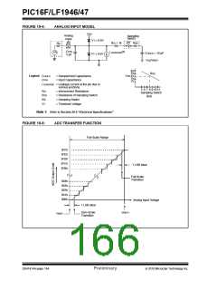
The input of the DAC can be connected to:
• External VREF pins
• Configuring the DACPSS bits to the proper
positive source.
• VDD supply voltage
• FVR (Fixed Voltage Reference)
• Configuring the DACR<4:0>x bits to ‘11111’ in
the DACCON1 register.
The output of the DAC can be configured to supply a
reference voltage to the following:
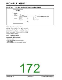
This is also the method used to output the voltage level
from the FVR to an output pin. See Section 16.4 “DAC
Voltage Reference Output” for more information.
• Comparator positive input
• ADC input channel
• DACOUT pin
Reference Figure 16-1 for output clamping examples.
The Digital-to-Analog Converter (DAC) can be enabled
by setting the DACEN bit of the DACCON0 register.
16.3.2
OUTPUT CLAMPED TO NEGATIVE
VOLTAGE SOURCE
The DAC output voltage can be set to VSRC- with the
least amount of power consumption by performing the
following:
16.1 Output Voltage Selection
The DAC has 32 voltage level ranges. The 32 levels
are set with the DACR<4:0> bits of the DACCON1
register.
• Clearing the DACEN bit in the DACCON0 register.
• Clearing the DACLPS bit in the DACCON0 register.
The DAC output voltage is determined by the following
equations:
• Configuring the DACNSS bits to the proper
negative source.
• Configuring the DACR<4:0> bits to ‘00000’ in the
DACCON1 register.
EQUATION 16-1: DAC OUTPUT VOLTAGE
DACR<4:0>
+ VSRC-
This allows the comparator to detect a zero-crossing
while not consuming additional current through the DAC
module.
VOUT = VSOURCE+ – VSOURCE- ------------------------------
5
2
Note:
VSOURCE+ can equal FVR Buffer 2, VDD or
VREF+. VSOURCE- can equal VSS or VREF-.
Reference Figure 16-1 for output clamping examples.
16.2 Ratiometric Output Level
The DAC output value is derived using a resistor ladder
with each end of the ladder tied to a positive and
negative voltage reference input source. If the voltage
of either input source fluctuates, a similar fluctuation will
result in the DAC output value.
The value of the individual resistors within the ladder
can be found in Section 29.0 “Electrical
Specifications”.
16.3 Low-Power Voltage State
In order for the DAC module to consume the least
amount of power, one of the two voltage reference input
sources to the resistor ladder must be disconnected.
Either the positive voltage source, (VSRC+), or the
negative voltage source, (VSRC-) can be disabled.
The negative voltage source is disabled by setting the
DACLPS bit in the DACCON0 register. Clearing the
DACLPS bit in the DACCON0 register disables the
positive voltage source.
2010 Microchip Technology Inc.
Preliminary
DS41414A-page 167

 MICROCHIP [ MICROCHIP ]