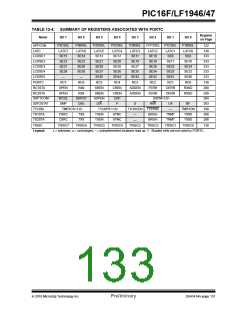
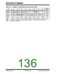
PIC16F/LF1946/47
12.6.2
PORTE FUNCTIONS AND OUTPUT
PRIORITIES
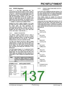
12.6 PORTE Registers
PORTE is
a 4-bit wide, bidirectional port. The
Each PORTE pin is multiplexed with other functions. The
pins, their combined functions and their output priorities
are briefly described here. For additional information,
refer to the appropriate section in this data sheet.
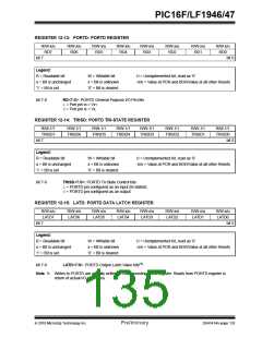
corresponding data direction register is TRISE. Setting a
TRISE bit (= 1) will make the corresponding PORTE pin
an input (i.e., put the corresponding output driver in a
High-Impedance mode). Clearing a TRISE bit (= 0) will
make the corresponding PORTE pin an output (i.e.,
enable the output driver and put the contents of the
output latch on the selected pin). The exception is RE3,
which is input only and its TRIS bit will always read as
‘1’. Example 12-5 shows how to initialize PORTE.
When multiple outputs are enabled, the actual pin
control goes to the peripheral with the lowest number in
the following lists.
Analog input and some digital input functions are not
included in the list below. These input functions can
remain active when the pin is configured as an output.
Certain digital input functions, such as the EUSART RX
signal, override other port functions and are included in
the priority list.
Reading the PORTE register (Register 12-16) reads
the status of the pins, whereas writing to it will write to
the PORT latch. All write operations are
read-modify-write operations. Therefore, a write to a
port implies that the port pins are read, this value is
modified and then written to the PORT data latch
(LATE). RE3 reads ‘0’ when MCLRE = 1.
RE0
1. P2D (CCP)
2. VLCD1 (LCD)
12.6.1
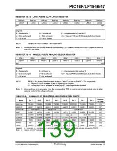
ANSELE REGISTER
RE1
The ANSELE register (Register 12-19) is used to
configure the Input mode of an I/O pin to analog.
Setting the appropriate ANSELE bit high will cause all
digital reads on the pin to be read as ‘0’ and allow
analog functions on the pin to operate correctly.
1. P2C (CCP)
2. VLCD2 (LCD)
RE2
1. P2B (CCP)
The state of the ANSELE bits has no affect on digital
output functions. A pin with TRIS clear and ANSEL set
will still operate as a digital output, but the Input mode
will be analog. This can cause unexpected behavior
when executing read-modify-write instructions on the
affected port.
2. VLCD3 (LCD)
RE3
1. P3C (CCP)
2. COM0 (LCD)
RE4
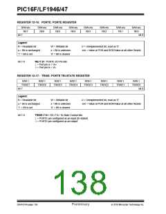
The TRISE register (Register 12-17) controls the PORTE
pin output drivers, even when they are being used as
analog inputs. The user should ensure the bits in the
TRISE register are maintained set when using them as
analog inputs. I/O pins configured as analog input always
read ‘0’.
1. P3B (CCP)
2. COM1 (LCD)
RE5
1. P1C (CCP)
2. COM32(LCD)
Note:
The ANSELE register must be initialized to
configure an analog channel as a digital
input. Pins configured as analog inputs will
read ‘0’.
RE6
1. P1B (CCP)
2. COM3 (LCD)
RE7
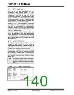
EXAMPLE 12-5:
INITIALIZING PORTE
1. CCP2/P2A (CCP)
2. SEG31 (LCD)
BANKSELPORTE
;
CLRF
BANKSEL LATE
CLRF LATE
BANKSELANSELE
CLRF ANSELE
BANKSELTRISE
PORTE
;Init PORTE
;Data Latch
;
;
;digital I/O
;
MOVLW
MOVWF
B‘00001100’ ;Set RE<3:2> as inputs
TRISE
;and set RE<1:0>
;as outputs
2010 Microchip Technology Inc.
Preliminary
DS41414A-page 135

 MICROCHIP [ MICROCHIP ]