PIC16F/LF1946/47
11.4 Modifying Flash Program Memory
11.5 User ID, Device ID and
Configuration Word Access
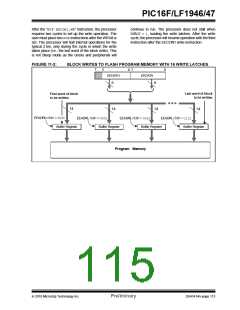
When modifying existing data in a program memory
row, and data within that row must be preserved, it must
first be read and saved in a RAM image. Program
memory is modified using the following steps:
Instead of accessing program memory or EEPROM
data memory, the User ID’s, Device ID/Revision ID and
Configuration Words can be accessed when CFGS = 1
in the EECON1 register. This is the region that would
be pointed to by PC<15> = 1, but not all addresses are
accessible. Different access may exist for reads and
writes. Refer to Table 11-2.
1. Load the starting address of the row to be
modified.
2. Read the existing data from the row into a RAM
image.
When read access is initiated on an address outside the
parameters listed in Table 11-2, the EEDATH:EEDATL
register pair is cleared.
3. Modify the RAM image to contain the new data
to be written into program memory.
4. Load the starting address of the row to be
rewritten.
5. Erase the program memory row.
6. Load the write latches with data from the RAM
image.
7. Initiate a programming operation.
8. Repeat steps 6 and 7 as many times as required
to reprogram the erased row.
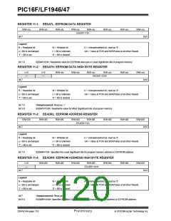
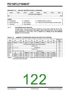
TABLE 11-2: USER ID, DEVICE ID AND CONFIGURATION WORD ACCESS (CFGS = 1)
Address
Function
Read Access
Write Access
8000h-8003h
8006h
User IDs
Yes
Yes
Yes
Yes
No
No
Device ID/Revision ID
Configuration Words 1 and 2
8007h-8008h
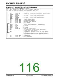
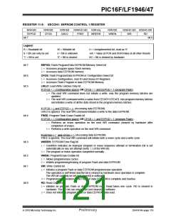
EXAMPLE 11-3: CONFIGURATION WORD AND DEVICE ID ACCESS
* This code block will read 1 word of program memory at the memory address:
*
*
PROG_ADDR_LO (must be 00h-08h) data will be returned in the variables;
PROG_DATA_HI, PROG_DATA_LO
BANKSEL EEADRL
; Select correct Bank
;
; Store LSB of address
; Clear MSB of address
MOVLW
MOVWF
CLRF
PROG_ADDR_LO
EEADRL
EEADRH
BSF
BCF
BSF
NOP
NOP
BSF
EECON1,CFGS
INTCON,GIE
EECON1,RD
; Select Configuration Space
; Disable interrupts
; Initiate read
; Executed (See Figure 11-1)
; Ignored (See Figure 11-1)
; Restore interrupts
INTCON,GIE
MOVF
EEDATL,W
; Get LSB of word
MOVWF
MOVF
PROG_DATA_LO
EEDATH,W
; Store in user location
; Get MSB of word
MOVWF
PROG_DATA_HI
; Store in user location
DS41414A-page 116
Preliminary
2010 Microchip Technology Inc.

 MICROCHIP [ MICROCHIP ]