PIC16F/LF1946/47
The following steps should be completed to load the
write latches and program a block of program memory.
These steps are divided into two parts. First, all write
latches are loaded with data except for the last program
memory location. Then, the last write latch is loaded
and the programming sequence is initiated. A special
unlock sequence is required to load a write latch with
data or initiate a Flash programming operation. This
unlock sequence should not be interrupted.
11.3.2
ERASING FLASH PROGRAM
MEMORY
While executing code, program memory can only be
erased by rows. To erase a row:
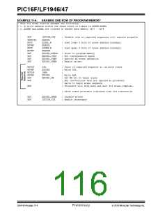
1. Load the EEADRH:EEADRL register pair with
the address of new row to be erased.
2. Clear the CFGS bit of the EECON1 register.
3. Set the EEPGD, FREE, and WREN bits of the
EECON1 register.
1. Set the EEPGD and WREN bits of the EECON1
register.
4. Write 55h, then AAh, to EECON2 (Flash
programming unlock sequence).
2. Clear the CFGS bit of the EECON1 register.
5. Set control bit WR of the EECON1 register to
begin the erase operation.
3. Set the LWLO bit of the EECON1 register. When
the LWLO bit of the EECON1 register is ‘1’, the
write sequence will only load the write latches
and will not initiate the write to Flash program
memory.
6. Poll the FREE bit in the EECON1 register to
determine when the row erase has completed.
See Example 11-4.
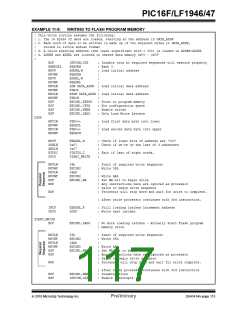
4. Load the EEADRH:EEADRL register pair with
the address of the location to be written.
After the “BSF EECON1,WR” instruction, the processor
requires two cycles to set up the erase operation. The
user must place two NOPinstructions after the WR bit is
set. The processor will halt internal operations for the
typical 2 ms erase time. This is not Sleep mode as the
clocks and peripherals will continue to run. After the
erase cycle, the processor will resume operation with
the third instruction after the EECON1 write instruction.
5. Load the EEDATH:EEDATL register pair with
the program memory data to be written.
6. Write 55h, then AAh, to EECON2, then set the
WR bit of the EECON1 register (Flash
programming unlock sequence). The write latch
is now loaded.
7. Increment the EEADRH:EEADRL register pair
to point to the next location.
11.3.3
WRITING TO FLASH PROGRAM
MEMORY
8. Repeat steps 5 through 7 until all but the last
write latch has been loaded.
Program memory is programmed using the following
steps:
9. Clear the LWLO bit of the EECON1 register.
When the LWLO bit of the EECON1 register is
‘0’, the write sequence will initiate the write to
Flash program memory.
1. Load the starting address of the word(s) to be
programmed.
2. Load the write latches with data.
10. Load the EEDATH:EEDATL register pair with
the program memory data to be written.
3. Initiate a programming operation.
4. Repeat steps 1 through 3 until all data is written.
11. Write 55h, then AAh, to EECON2, then set the
WR bit of the EECON1 register (Flash
programming unlock sequence). The entire
latch block is now written to Flash program
memory.
Before writing to program memory, the word(s) to be
written must be erased or previously unwritten. Pro-
gram memory can only be erased one row at a time. No
automatic erase occurs upon the initiation of the write.
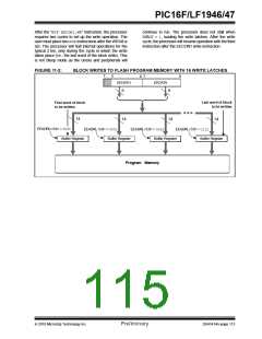
Program memory can be written one or more words at
a time. The maximum number of words written at one
time is equal to the number of write latches. See
Figure 11-2 (block writes to program memory with 16
write latches) for more details. The write latches are
aligned to the address boundary defined by EEADRL
as shown in Table 11-1. Write operations do not cross
these boundaries. At the completion of a program
memory write operation, the write latches are reset to
contain 0x3FFF.
It is not necessary to load the entire write latch block
with user program data. However, the entire write latch
block will be written to program memory.
An example of the complete write sequence for eight
words is shown in Example 11-5. The initial address is
loaded into the EEADRH:EEADRL register pair; the
eight words of data are loaded using indirect
addressing.
Note:
The code sequence provided in
Example 11-5 must be repeated multiple
times to fully program an erased program
memory row.
DS41414A-page 112
Preliminary
2010 Microchip Technology Inc.

 MICROCHIP [ MICROCHIP ]