PIC16F/LF1946/47
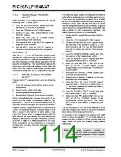
After the “BSF EECON1,WR” instruction, the processor
requires two cycles to set up the write operation. The
user must place two NOPinstructions after the WR bit is
set. The processor will halt internal operations for the
typical 2 ms, only during the cycle in which the write
takes place (i.e., the last word of the block write). This
is not Sleep mode as the clocks and peripherals will
continue to run. The processor does not stall when
LWLO = 1, loading the write latches. After the write
cycle, the processor will resume operation with the third
instruction after the EECON1 write instruction.
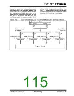
FIGURE 11-2:
BLOCK WRITES TO FLASH PROGRAM MEMORY WITH 16 WRITE LATCHES
7
5
0
0 7
EEDATH
6
EEDATA
8
Last word of block
to be written
First word of block
to be written
14
14
14
14
EEADRL<3:0> = 0000
EEADRL<3:0> = 0001
Buffer Register
EEADRL<3:0> = 0010
EEADRL<3:0> = 1111
Buffer Register
Buffer Register
Buffer Register
Program Memory
2010 Microchip Technology Inc.
Preliminary
DS41414A-page 113

 MICROCHIP [ MICROCHIP ]