PIC16F/LF1946/47
11.3.1
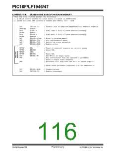
READING THE FLASH PROGRAM
MEMORY
11.3 Flash Program Memory Overview
It is important to understand the Flash program mem-
ory structure for erase and programming operations.
Flash Program memory is arranged in rows. A row con-
sists of a fixed number of 14-bit program memory
words. A row is the minimum block size that can be
erased by user software.
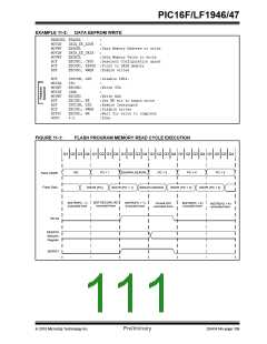
To read a program memory location, the user must:
1. Write the Least and Most Significant address
bits to the EEADRH:EEADRL register pair.
2. Clear the CFGS bit of the EECON1 register.
3. Set the EEPGD control bit of the EECON1
register.
Flash program memory may only be written or erased
if the destination address is in a segment of memory
that is not write-protected, as defined in bits WRT<1:0>
of Configuration Word 2.
4. Then, set control bit RD of the EECON1 register.
Once the read control bit is set, the program memory
Flash controller will use the second instruction cycle to
read the data. This causes the second instruction
immediately following the “BSF EECON1,RD” instruction
to be ignored. The data is available in the very next cycle,
in the EEDATH:EEDATL register pair; therefore, it can
be read as two bytes in the following instructions.
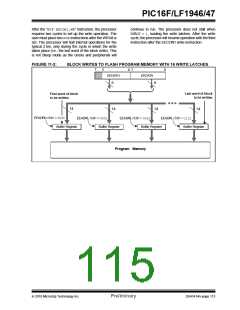
After a row has been erased, the user can reprogram
all or a portion of this row. Data to be written into the
program memory row is written to 14-bit wide data write
latches. These write latches are not directly accessible
to the user, but may be loaded via sequential writes to
the EEDATH:EEDATL register pair.
EEDATH:EEDATL register pair will hold this value until
another read or until it is written to by the user.
Note:
If the user wants to modify only a portion
of a previously programmed row, then the
contents of the entire row must be read
and saved in RAM prior to the erase.
Note 1: The two instructions following a program
memory read are required to be NOPs.
This prevents the user from executing a
two-cycle instruction on the next
instruction after the RD bit is set.
The number of data write latches is not equivalent to
the number of row locations. During programming, user
software will need to fill the set of write latches and ini-
tiate a programming operation multiple times in order to
fully reprogram an erased row. For example, a device
with a row size of 32 words and eight write latches will
need to load the write latches with data and initiate a
programming operation four times.
2: Flash program memory can be read
regardless of the setting of the CP bit.
The size of a program memory row and the number of
program memory write latches may vary by device.
See Table 11-1 for details.
TABLE 11-1: FLASH MEMORY ORGANIZATION BY DEVICE
Device
Erase Block (Row) Size/Boundary
Number of Write Latches/Boundary
PIC16F/LF1946/47
32 words, EEADRL<4:0> = 00000
8 words, EEADRL<2:0> = 000
DS41414A-page 110
Preliminary
2010 Microchip Technology Inc.

 MICROCHIP [ MICROCHIP ]