PIC16F/LF1946/47
11.2.2
WRITING TO THE DATA EEPROM
MEMORY
11.2 Using the Data EEPROM
The data EEPROM is a high-endurance, byte address-
able array that has been optimized for the storage of
frequently changing information (e.g., program vari-
ables or other data that are updated often). When vari-
ables in one section change frequently, while variables
in another section do not change, it is possible to
exceed the total number of write cycles to the
EEPROM without exceeding the total number of write
cycles to a single byte. Refer to Section 29.0 “Electri-
cal Specifications”. If this is the case, then a refresh
of the array must be performed. For this reason, vari-
ables that change infrequently (such as constants, IDs,
calibration, etc.) should be stored in Flash program
memory.
To write an EEPROM data location, the user must first
write the address to the EEADRL register and the data
to the EEDATL register. Then the user must follow a
specific sequence to initiate the write for each byte.
The write will not initiate if the above sequence is not
followed exactly (write 55h to EECON2, write AAh to
EECON2, then set the WR bit) for each byte. Interrupts
should be disabled during this code segment.
Additionally, the WREN bit in EECON1 must be set to
enable write. This mechanism prevents accidental
writes to data EEPROM due to errant (unexpected)
code execution (i.e., lost programs). The user should
keep the WREN bit clear at all times, except when
updating EEPROM. The WREN bit is not cleared
by hardware.
11.2.1
READING THE DATA EEPROM
MEMORY
After a write sequence has been initiated, clearing the
WREN bit will not affect this write cycle. The WR bit will
be inhibited from being set unless the WREN bit is set.
To read a data memory location, the user must write the
address to the EEADRL register, clear the EEPGD and
CFGS control bits of the EECON1 register, and then
set control bit RD. The data is available at the very next
cycle, in the EEDATL register; therefore, it can be read
in the next instruction. EEDATL will hold this value until
another read or until it is written to by the user (during
a write operation).
At the completion of the write cycle, the WR bit is
cleared in hardware and the EE Write Complete
Interrupt Flag bit (EEIF) is set. The user can either
enable this interrupt or poll this bit. EEIF must be
cleared by software.
11.2.3
PROTECTION AGAINST SPURIOUS
WRITE
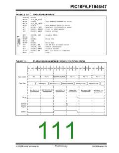
EXAMPLE 11-1:
DATA EEPROM READ
BANKSELEEADRL
;
There are conditions when the user may not want to
write to the data EEPROM memory. To protect against
spurious EEPROM writes, various mechanisms have
been built-in. On power-up, WREN is cleared. Also, the
Power-up Timer (64 ms duration) prevents EEPROM
write.
MOVLW
MOVWF
DATA_EE_ADDR ;
EEADRL
;Data Memory
;Address to read
EECON1, CFGS ;Deselect Config space
EECON1, EEPGD;Point to DATA memory
BCF
BCF
BSF
MOVF
EECON1, RD
EEDATL, W
;EE Read
;W = EEDATL
The write initiate sequence and the WREN bit together
help prevent an accidental write during:
• Brown-out
Note:
Data EEPROM can be read regardless of
the setting of the CPD bit.
• Power Glitch
• Software Malfunction
11.2.4
DATA EEPROM OPERATION
DURING CODE-PROTECT
Data memory can be code-protected by programming
the CPD bit in the Configuration Word 1 (Register 4-1)
to ‘0’.
When the data memory is code-protected, only the
CPU is able to read and write data to the data
EEPROM. It is recommended to code-protect the pro-
gram memory when code protecting data memory. This
prevents anyone from replacing your program with a
program that will access the contents of the data
EEPROM.
DS41414A-page 108
Preliminary
2010 Microchip Technology Inc.

 MICROCHIP [ MICROCHIP ]