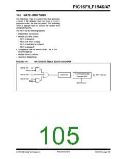
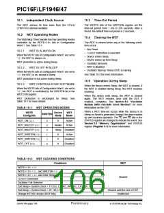
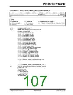
PIC16F/LF1946/47
11.1 EEADRL and EEADRH Registers
11.0 DATA EEPROM AND FLASH
PROGRAM MEMORY
CONTROL
The EEADRH:EEADRL register pair can address up to
a maximum of 256 bytes of data EEPROM or up to a
maximum of 32K words of program memory.
The Data EEPROM and Flash program memory are
readable and writable during normal operation (full VDD
range). These memories are not directly mapped in the
register file space. Instead, they are indirectly
addressed through the Special Function Registers
(SFRs). There are six SFRs used to access these
memories:
When selecting a program address value, the MSB of
the address is written to the EEADRH register and the
LSB is written to the EEADRL register. When selecting
a EEPROM address value, only the LSB of the address
is written to the EEADRL register.
11.1.1
EECON1 AND EECON2 REGISTERS
• EECON1
• EECON2
• EEDATL
• EEDATH
• EEADRL
• EEADRH
EECON1 is the control register for EE memory
accesses.
Control bit EEPGD determines if the access will be a
program or data memory access. When clear, any
subsequent operations will operate on the EEPROM
memory. When set, any subsequent operations will
operate on the program memory. On Reset, EEPROM is
selected by default.
When interfacing the data memory block, EEDATL
holds the 8-bit data for read/write, and EEADRL holds
the address of the EEDATL location being accessed.
These devices have 256 bytes of data EEPROM with
an address range from 0h to 0FFh.
Control bits RD and WR initiate read and write,
respectively. These bits cannot be cleared, only set, in
software. They are cleared in hardware at completion
of the read or write operation. The inability to clear the
WR bit in software prevents the accidental, premature
termination of a write operation.
When accessing the program memory block, the EED-
ATH:EEDATL register pair forms a 2-byte word that
holds the 14-bit data for read/write, and the EEADRL
and EEADRH registers form a 2-byte word that holds
the 15-bit address of the program memory location
being read.
The WREN bit, when set, will allow a write operation to
occur. On power-up, the WREN bit is clear. The
WRERR bit is set when a write operation is interrupted
by a Reset during normal operation. In these situations,
following Reset, the user can check the WRERR bit
and execute the appropriate error handling routine.
The EEPROM data memory allows byte read and write.
An EEPROM byte write automatically erases the loca-
tion and writes the new data (erase before write).
Interrupt flag bit EEIF of the PIR2 register is set when
write is complete. It must be cleared in the software.
The write time is controlled by an on-chip timer. The
write/erase voltages are generated by an on-chip
charge pump rated to operate over the voltage range of
the device for byte or word operations.
Reading EECON2 will read all ‘0’s. The EECON2 reg-
ister is used exclusively in the data EEPROM write
sequence. To enable writes, a specific pattern must be
written to EECON2.
Depending on the setting of the Flash Program
Memory Self Write Enable bits WRT<1:0> of the
Configuration Word 2, the device may or may not be
able to write certain blocks of the program memory.
However, reads from the program memory are always
allowed.
When the device is code-protected, the device
programmer can no longer access data or program
memory. When code-protected, the CPU may continue
to read and write the data EEPROM memory and Flash
program memory.
2010 Microchip Technology Inc.
Preliminary
DS41414A-page 107

 MICROCHIP [ MICROCHIP ]