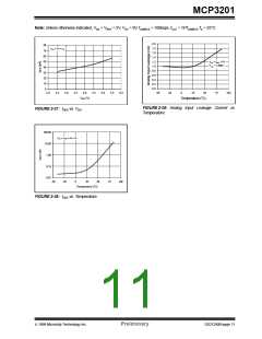
MCP3201
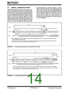
(the output is at high impedance for the first two clocks),
the null bit and the highest order five bits of the conver-
sion. After the second eight clocks have been sent to
the device, the MCU receive register will contain the
lowest order seven bits and the B1 bit repeated as the
A/D Converter has begun to shift out LSB first data with
the extra clock. Typical procedure would then call for
the lower order byte of data to be shifted right by one bit
to remove the extra B1 bit. The B7 bit is then trans-
ferred from the high order byte to the lower order byte,
and then the higher order byte is shifted one bit to the
right as well. Easier manipulation of the converted data
can be obtained by using this method.
6.0
APPLICATIONS INFORMATION
6.1
Using the MCP3201 with
Microcontroller SPI Ports
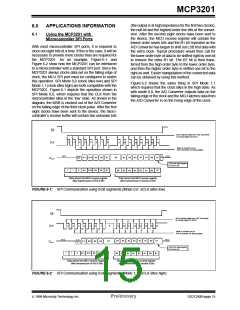
With most microcontroller SPI ports, it is required to
clock out eight bits at a time. If this is the case, it will be
necessary to provide more clocks than are required for
the MCP3201. As an example, Figure 6-1 and
Figure 6-2 show how the MCP3201 can be interfaced
to a microcontroller with a standard SPI port. Since the
MCP3201 always clocks data out on the falling edge of
clock, the MCU SPI port must be configured to match
this operation. SPI Mode 0,0 (clock idles low) and SPI
Mode 1,1 (clock idles high) are both compatible with the
MCP3201. Figure 6-1 depicts the operation shown in
SPI Mode 0,0, which requires that the CLK from the
microcontroller idles in the ‘low’ state. As shown in the
diagram, the MSB is clocked out of the A/D Converter
on the falling edge of the third clock pulse. After the first
eight clocks have been sent to the device, the micro-
controller’s receive buffer will contain two unknown bits
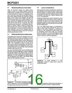
Figure 6-2 shows the same thing in SPI Mode 1,1
which requires that the clock idles in the high state. As
with mode 0,0, the A/D Converter outputs data on the
falling edge of the clock and the MCU latches data from
the A/D Converter in on the rising edge of the clock.
CS
MCU latches data from A/D Converter
on rising edges of SCLK
1
2
3
4
5
6
7
8
CLK
9
10
11
12
13
14
15
16
Data is clocked out of
A/D Converter on falling edges
HI-Z
HI-Z
NULL
BIT
B2
B6
B5
B5
B4
B4
B3
B3
B2
B2
B1
B1
B0
B0
B1
B1
B11 B10 B9
B8
B8
B7
B7
DOUT
LSB first data begins
to come out
?
?
0
B11 B10 B9
B6
Data stored into MCU receive register
after transmission of first 8 bits
Data stored into MCU receive register
after transmission of second 8 bits
FIGURE 6-1: SPI Communication using 8-bit segments (Mode 0,0: SCLK idles low).
CS
MCU latches data from A/D Converter
on rising edges of SCLK
8
1
2
3
4
5
6
7
CLK
9
10
11
B4
12
B3
13
14
B1
15
16
Data is clocked out of
A/D Converter on falling edges
HI-Z
HI-Z
NULL
BIT
B6
B5
B2
B0
B1
B1
B11 B10 B9
B8
B7
DOUT
LSB first data begins
to come out
?
?
0
B11 B10 B9
B8
B7
B6
B5
B4
B3
B2
B1
B0
Data stored into MCU receive register
after transmission of first 8 bits
Data stored into MCU receive register
after transmission of second 8 bits
FIGURE 6-2: SPI Communication using 8-bit segments (Mode 1,1: SCLK idles high).
1999 Microchip Technology Inc.
Preliminary
DS21290B-page 15

 MICROCHIP [ MICROCHIP ]