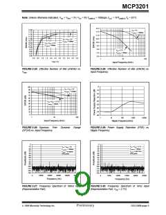
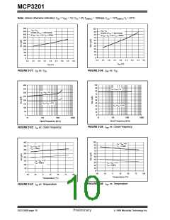
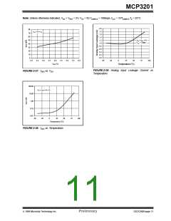
MCP3201
VDD
Sampling
Switch
VT = 0.6V
VT = 0.6V
RSS = 1kΩ
CHx
SS
RS
CSAMPLE
= DAC capacitance
= 20 pF
CPIN
7pF
ILEAKAGE
±1nA
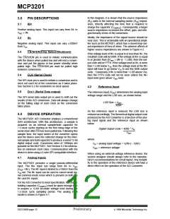
VA
VSS
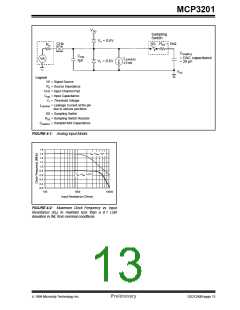
Legend
VA = Signal Source
RS = Source Impedance
CHx = Input Channel Pad
CPIN = Input Capacitance
VT = Threshold Voltage
ILEAKAGE = Leakage Current at the pin
due to various junctions
SS = Sampling Switch
RSS = Sampling Switch Resistor
CSAMPLE = Sample/Hold Capacitance
FIGURE 4-1: Analog Input Model.
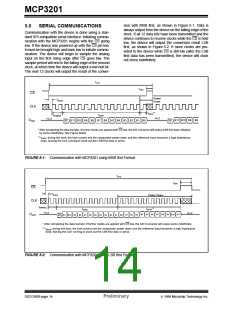
1.8
VDD = VREF = 5V
1.6
1.4
1.2
1.0
0.8
0.6
0.4
0.2
0.0
VDD = VREF = 2.7V
100
1000
Input Resistance (Ohms)
10000
FIGURE 4-2: Maximum Clock Frequency vs. Input
Resistance (RS) to maintain less than a 0.1 LSB
deviation in INL from nominal conditions.
1999 Microchip Technology Inc.
Preliminary
DS21290B-page 13

 MICROCHIP [ MICROCHIP ]