MCP3201
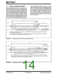
sion with MSB first, as shown in Figure 5-1. Data is
always output from the device on the falling edge of the
clock. If all 12 data bits have been transmitted and the
device continues to receive clocks while the CS is held
low, the device will output the conversion result LSB
first, as shown in Figure 5-2. If more clocks are pro-
vided to the device while CS is still low (after the LSB
first data has been transmitted), the device will clock
out zeros indefinitely.
5.0
SERIAL COMMUNICATIONS
Communication with the device is done using a stan-
dard SPI-compatible serial interface. Initiating commu-
nication with the MCP3201 begins with the CS going
low. If the device was powered up with the CS pin low,
it must be brought high and back low to initiate commu-
nication. The device will begin to sample the analog
input on the first rising edge after CS goes low. The
sample period will end in the falling edge of the second
clock, at which time the device will output a low null bit.
The next 12 clocks will output the result of the conver-
tCYC
tCSH
CS
Power
Down
tSUCS
CLK
tDATA**
tCONV
B11 B10 B9 B8 B7 B6 B5 B4 B3 B2 B1 B0*
tSAMPLE
HI-Z
HI-Z
NULL
BIT
NULL
BIT
DOUT
B11 B10 B9 B8
* After completing the data transfer, if further clocks are applied with CS low, the A/D Converter will output LSB first data, followed
by zeros indefinitely. See Figure below.
** tDATA: during this time, the bias current and the comparator power down and the reference input becomes a high impedance
node, leaving the CLK running to clock out the LSB-first data or zeros.
FIGURE 5-1: Communication with MCP3201 using MSB first Format.
tCYC
tCSH
CS
tSUCS
Power Down
CLK
tSAMPLE
tDATA**
tCONV
HI-Z
HI-Z
NULL
BIT
DOUT
B4 B5 B6 B7 B8 B9 B10 B11*
B1 B2 B3
B11 B10 B9 B8 B7 B6 B5 B4 B3 B2 B1 B0
* After completing the data transfer, if further clocks are applied with CS low, the A/D Converter will output zeros indefinitely.
** tDATA: during this time, the bias current and the comparator power down and the reference input becomes a high impedance
node, leaving the CLK running to clock out the LSB-first data or zeros.
FIGURE 5-2: Communication with MCP3201 using LSB first Format.
DS21290B-page 14
Preliminary
1999 Microchip Technology Inc.

 MICROCHIP [ MICROCHIP ]