MCP3201
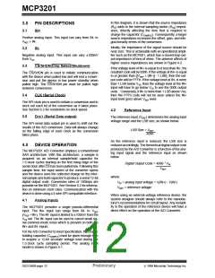
In this diagram, it is shown that the source impedance
(RS) adds to the internal sampling switch (RSS) imped-
ance, directly affecting the time that is required to
charge the capacitor (CSAMPLE). Consequently, a larger
source impedance increases the offset, gain, and inte-
gral linearity errors of the conversion.
3.0
PIN DESCRIPTIONS
3.1
IN+
Positive analog input. This input can vary from IN- to
VREF + IN-.
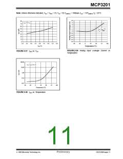
Ideally, the impedance of the signal source should be
near zero. This is achievable with an operational ampli-
fier such as the MCP601, which has a closed loop out-
put impedance of tens of ohms. The adverse affects of
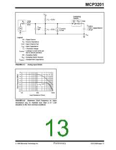
higher source impedances are shown in Figure 4-2.
3.2
IN-
Negative analog input. This input can vary ±100mV
from VSS.
3.3
CS/SHDN(Chip Select/Shutdown)
If the voltage level of IN+ is equal to or less than IN-, the
resultant code will be 000h. If the voltage at IN+ is equal
to or greater than {[VREF + (IN-)] - 1 LSB}, then the out-
put code will be FFFh. If the voltage level at IN- is more
than 1 LSB below VSS, then the voltage level at the IN+
input will have to go below VSS to see the 000h output
code. Conversely, if IN- is more than 1 LSB above Vss,
then the FFFh code will not be seen unless the IN+
input level goes above VREF level.
The CS/SHDN pin is used to initiate communication
with the device when pulled low and will end a conver-
sion and put the device in low power standby when
pulled high. The CS/SHDN pin must be pulled high
between conversions.
3.4
CLK (Serial Clock)
The SPI clock pin is used to initiate a conversion and to
clock out each bit of the conversion as it takes place.
See Section 6.2 for constraints on clock speed.
4.2
Reference Input
3.5
DOUT (Serial Data output)
The reference input (VREF) determines the analog input
voltage range and the LSB size, as shown below.
The SPI serial data output pin is used to shift out the
results of the A/D conversion. Data will always change
on the falling edge of each clock as the conversion
takes place.
LSB Size = VREF
4096
As the reference input is reduced, the LSB size is
reduced accordingly. The theoretical digital output code
produced by the A/D Converter is a function of the ana-
log input signal and the reference input as shown
below.
4.0
DEVICE OPERATION
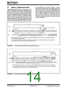
The MCP3201 A/D Converter employs a conventional
SAR architecture. With this architecture, a sample is
acquired on an internal sample/hold capacitor for
1.5 clock cycles starting on the first rising edge of the
serial clock after CS has been pulled low. Following this
sample time, the input switch of the converter opens
and the device uses the collected charge on the inter-
nal sample and hold capacitor to produce a serial 12-bit
digital output code. Conversion rates of 100ksps are
possible on the MCP3201. See Section 6.2 for informa-
tion on minimum clock rates. Communication with the
device is done using a 3-wire SPI-compatible interface.
Digital Output Code = 4096 * VIN
VREF
where:
VIN = analog input voltage = V(IN+) - V(IN-)
VREF = reference voltage
When using an external voltage reference device, the
system designer should always refer to the manufac-
turer’s recommendations for circuit layout. Any instabil-
ity in the operation of the reference device will have a
direct effect on the operation of the A/D Converter.
4.1
Analog Inputs
The MCP3201 provides a single pseudo-differential
input. The IN+ input can range from IN- to VREF
(VREF +IN-). The IN- input is limited to ±100mV from the
VSS rail. The IN- input can be used to cancel small sig-
nal common-mode noise which is present on both the
IN+ and IN- inputs.
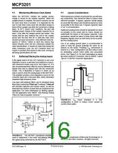
For the A/D Converter to meet specification, the charge
holding capacitor (CSAMPLE) must be given enough time
to acquire a 12-bit accurate voltage level during the
1.5 clock cycle sampling period. The analog input
model is shown in Figure 4-1.
DS21290B-page 12
Preliminary
1999 Microchip Technology Inc.

 MICROCHIP [ MICROCHIP ]