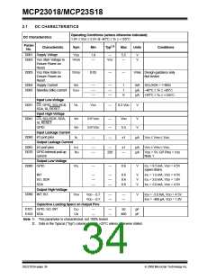
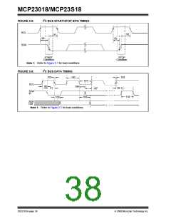
MCP23018/MCP23S18
2.1
DC CHARACTERISTICS
Operating Conditions (unless otherwise indicated):
1.8V ≤ VDD ≤ 5.5V at -40°C ≤ TA ≤ +125°C
DC Characteristics
Param
Characteristic
Sym
Min
Typ( 2)
Max
Units
Conditions
No.
D001 Supply Voltage
VDD
1.8
—
—
5.5
—
V
V
D002 VDD Start Voltage to
Ensure Power-on
Reset
VPOR
VSS
D003 VDD Rise Rate to
Ensure Power-on
Reset
SVDD
0.05
—
—
V/ms Design guidance only.
Not tested.
D004 Supply Current
IDD
—
—
—
—
—
—
1
1
6
mA
µA
µA
SCL/SCK = 1 MHz
–40°C ≤ TA ≤ +85°C
+85°C ≤ TA ≤ +125°C
D005 Standby (Idle) current
IDDS
Input Low-Voltage
D031 CS, GPIO, SCL/SCK,
SDA, SI, RESET
VIL
VSS
—
0.2 VDD
V
Input High-Voltage
D041 CS, SCL/SCK, SDA,
SI, RESET
VIH
VIH
0.8 VDD
0.8 VDD
—
—
VDD
5.5
V
V
GPIO
Input Leakage Current
D060 I/O port pins
IIL
—
—
±1
µA
VSS ≤ VPIN ≤ VDD,
VSS ≤ VPIN ≤ VDD,
Output Leakage Current
D065 I/O port pins
ILO
IPU
—
—
—
±1
—
µA
µA
D070 GPIO internal pull-up
current
220
VDD = 5V, GP Pins = VSS
Note 1
Output Low-Voltage
D080 GPIO
VOL
—
—
0.6
V
IOL = 8.5 mA, VDD = 4.5V
(open-drain)
INT
SO, SDA
—
—
—
—
—
—
0.6
0.6
0.8
V
V
V
IOL = 1.6 mA, VDD = 4.5V
IOL = 3.0 mA, VDD = 1.8V
IOL = 3.0 mA, VDD = 4.5V
SDA
Output High-Voltage
D090 INT, SO
VOH
VDD – 0.7
VDD – 0.7
—
—
—
—
V
IOH = -3.0 mA, VDD = 4.5V
IOH = -400 µA, VDD = 1.8V
Capacitive Loading Specs on Output Pins
D101 GPIO, SO, INT
D102 SDA
CIO
CB
—
—
—
—
50
pF
pF
400
Note 1: This parameter is characterized, not 100% tested.
2: Data in the Typical (“Typ”) column is at 5V, +25°C unless otherwise stated.
DS22103A-page 34
© 2008 Microchip Technology Inc.

 MICROCHIP [ MICROCHIP ]