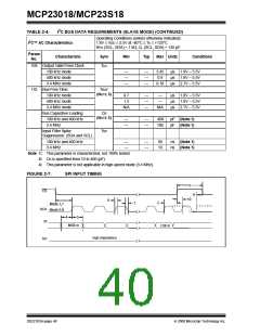
MCP23018/MCP23S18
TABLE 2-2:
GP AND INT PINS
AC Characteristics Standard Operating Conditions (unless otherwise specified)
1.8V ≤ VDD ≤ 5.5V at -40°C ≤ TA ≤ +125°C.
Parameter
No.
Sym
Characteristic
Min Typ( 2) Max Units
Conditions
50
51
52
53
54
tGPOV Serial data to output valid
tINTD Interrupt pin disable time
tGPIV GP input change to register valid
tGPINT IOC event to INT active
tGLITCH Glitch filter on GP pins
—
—
—
—
—
—
—
500
600
—
ns
ns
450
—
ns Note 1
ns
600
50
—
ns Note 1
Note 1: This parameter is characterized, not 100% tested.
2: Data in the Typical (“Typ”) column is at 5V, 25°C, unless otherwise stated.
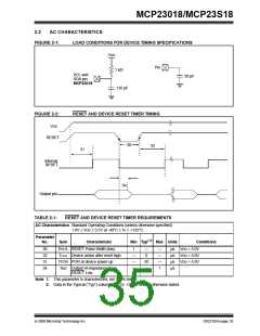
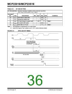
FIGURE 2-3:
GPIO AND INT TIMING
SCL
SDA
In
D1
D0
LSb of data byte zero
during a write or read
command, depending
on parameter
50
51
GPn
Output
Pin
INT
Pin
INT pin
inactive
INT pin active
53
GPn
Input
Pin
52
Register
Loaded
DS22103A-page 36
© 2008 Microchip Technology Inc.

 MICROCHIP [ MICROCHIP ]