MCP2021/2
1.5
Pin Descriptions
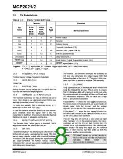
TABLE 1-1:
PINOUT DESCRIPTIONS
Devices
Function
8-Pin
DFN,
PDIP,
SOIC
14-Pin
PDIP,
SOIC,
TSSOP
Pin
Name
Pin
Type
Normal Operation
VREG
VSS
3
5
3
11
13
4
O
P
Power Output
Ground
VBB
7
P
Battery Supply
TXD
4
I
Transmit Data Input (TTL)
Receive Data Output (CMOS)
LIN bus (bidirectional)
RXD
1
1
O
LBUS
6
12
2
I/O
TTL
OD
OD
CS/LWAKE
FAULT/TXE
RESET
2
Chip Select (TTL)
8
14
5
Fault Detect Output, Transmitter Enable (OD)
RESET signal Output (OD)
—
Legend: TTL = TTL input buffer, ST = Schmitt Trigger input buffer, OD = Open-Drain output,
P = Power, O = Output, I = Input
The internal LIN Receiver observes the activities on
LIN bus, and generates the output signal RXD that
follows the state of the LBUS. A 1st degree 1 MHz, low-
pass input filter is placed to maintain EMI immunity.
1.5.1
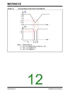
POWER OUTPUT (VREG)
Positive Supply Voltage Regulator Output pin.
1.5.2
GROUND (VSS)
BATTERY (VBB)
Ground pin.
1.5.3
1.5.7
CS/LWAKE
Chip Select Input pin. A internal pull-down resistor will
keep the CS/LWAKE pin low. This is done to ensure
that no disruptive data will be present on the bus while
the microcontroller is executing a Power-on Reset and
I/O initialization sequence. The pin must see a high
level to activate the transmitter.
Battery Positive Supply Voltage pin. This pin is also the
input for the internal voltage regulator.
1.5.4
TRANSMIT DATA INPUT (TXD)
The Transmit Data Input pin has an internal pull-up to
VREG. The LIN pin is low (dominant) when TXD is low,
and high (recessive) when TXD is high.
If CS/LWAKE= ‘0’ when the VBB supply is turned on,
the device stays in Ready mode (Low-power mode). In
Ready mode, both the receiver and the voltage
regulator are on and the LIN transmitter driver is off.
For extra bus security, TXD is internally forced to ‘1’
when VREG is less than 1.8V (typ.).
In case the thermal protection detects an over-temper-
ature condition while the signal TXD is low, the
transmitter is shutdown. The recovery from the thermal
shutdown is equal to adequate cooling time.
If CS/LWAKE = ‘1’ when the VBB supply is turned on,
the device will proceed to the Operation mode as soon
as the VREG output has stabilised.
This pin may also be used as a local wake-up input
(See Example 1-1). In this implementation, the micro-
controller will set the I/O pin that controls the CS/
LWAKE as an high-impedance input. The internal pull-
down resistor will keep the input low. An external
switch, or other source, can then wake-up both the
transceiver and the microcontroller.
1.5.5
RECEIVE DATA OUTPUT (RXD)
The Receive Data Output pin is a standard CMOS
output and follows the state of the LIN pin.
1.5.6
LIN BUS
The bidirectional LIN bus Interface pin is the driver unit
for the LIN pin and is controlled by the signal TXD. LIN
has an open collector output with a current limitation.
To reduce EMI, the edges during the signal changes
are slope-controlled. To further reduce radiated
emissions, the LBUS pin has corner-rounding control for
both falling and rising edges.
Note:
CS/LWAKE should not be tied directly to
VREG as this could force the MCP202x into
Operation
Mode
before
the
microcontroller is initialized.
DS22018E-page 8
© 2009 Microchip Technology Inc.

 MICROCHIP [ MICROCHIP ]