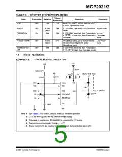
MCP2021/2
1.3.4
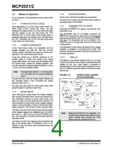
OPERATION MODE
1.3
Modes of Operation
In this mode, all internal modules are operational.
For an overview of all operational modes, please refer
to Table 1-1.
The MCP2021/2 will go into the Power-down mode on
the falling edge of CS/LWAKE.
1.3.1
POWER-ON-RESET MODE
1.3.5
TRANSMITTER OFF MODE
Upon application of VBB, the device enters Power-On-
Reset mode (POR). During this mode, the part
maintains the digital section in a reset mode and waits
until the voltage on pin VBB rises above the “ON”
threshold (Typ. 5.75V) to enter to the Ready mode. If
during the operation, the voltage on pin VBB falls below
the “OFF” threshold (Typ. 4.25V), the part comes back
to the Power-On-Reset mode.
Whenever the FAULT/TXE signal is low and the LBUS
transmitter is off.
The transmitter may be re-enabled whenever the
FAULT/TXE signal returns high, either by removing the
internal fault condition or the CPU returning the FAULT/
TXE high. The transmitter will not be enabled if the
FAULT/TXE pin is brought high when the internal fault
is still present.
1.3.2
POWER-DOWN MODE
The transmitter is also turned off whenever the voltage
regulator is unstable or recovering from a fault. This
prevents unwanted disruption of the bus during times of
uncertain operation.
In the Power-down mode, the transmitter and the
voltage regulator are both off. Only the receiver
section, and the CS/LWAKE pin wake-up circuits are in
operation. This is the lowest power mode.
If any bus activity (e.g. a BREAK character) or CS/
LWAKE going to a high level should occur during
Power-down mode, the device will immediately enter
the Ready mode, enable the voltage regulator, and
once the output has stabilized (approximately 0.3 ms to
1.2 ms), go to the Operation mode.
1.3.5.1
Wake-up
The Wake-up sub module observes the LBUS in order
to detect bus activity. Bus activity is detected when the
voltage on the LBUS stays below a threshold of
approximately 3V for at least a typical duration of 10 µs.
Such a condition causes the device to leave the Power-
down mode.
Note:
The above time interval < 1.2 ms assumes
12V VBB input and no thermal shutdown
event.
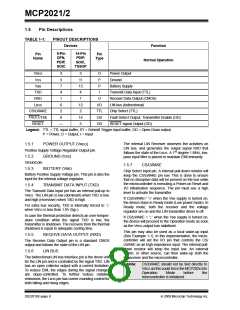
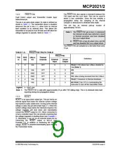
FIGURE 1-2:
OPERATIONAL MODES
STATE DIAGRAMS
The part will also enter the Ready mode, followed by
the Operation mode, if the CS/LWAKE pin should
become active true (‘1’).
CS/LWAKE
= false
Power-down
Bus Activity
OR
Mode
CS/LWAKE = true
The part may only enter the Power-down mode after
going through an Operation mode step.
CS/LWAKE
= false
Transmitter
Off
Mode
1.3.3
READY MODE
VBBOK = true
Operation
Mode
Ready
Mode
Upon entering the Ready mode, the voltage regulator
and receiver threshold detect circuit are powered up.
The transmitter remains in power down mode. The
device is ready to receive data but not to transmit. If a
microcontroller is being driven by the voltage regulator
output, it will go through a Power-on Reset and initial-
ization sequence. The LIN pin is in the recessive state.
FAULT/TXE
= false
FAULT/TXE = true
VREGOK = true
POR
AND
CS/LWAKE = true
Start
The device will stay in the Ready mode until the output
of the voltage regulator has stabilized and CS/LWAKE
pin is true (‘1’). After VREG is OK and CS/LWAKE pin is
true, the transmitter is enabled and the part enters the
Operation mode.
Note:
While the MCP2021/2 is in shutdown, TXD
should not be actively driven high or it may
power internal logic through the ESD
diodes and may damage the device.
On Power-on of the VBB supply pin, the component will
stay in the Ready mode if CS/LWAKE is low. If CS/
LWAKE is high, the device will immediately enter the
Operation mode.
DS22018E-page 4
© 2009 Microchip Technology Inc.

 MICROCHIP [ MICROCHIP ]