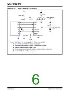
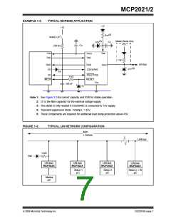
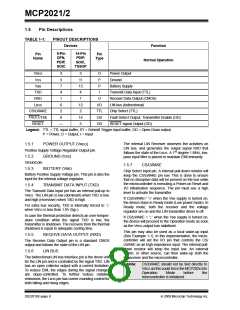
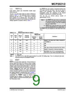
MCP2021/2
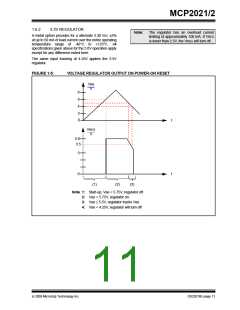
When the input voltage (VBB) drops below the
differential needed to provide stable regulation, the
output VREG) will track the input down to approximately
+4.25V. The regulator will turn off the output at this
point. This will allow PIC® microcontrollers, with
internal POR circuits, to generate a clean arming of the
Power-on Reset trip point. The regulator output will
1.6
Internal Voltage Regulator
1.6.1
5.0V REGULATOR
The MCP2021 has a low-drop-out voltage, positive
regulator capable of supplying 5.00 VDC ±3% at up to
50 mA of load current over the entire operating
temperature range of -40°C to +125°C. With a load
current of 50 mA, the minimum input to output voltage
differential required for the output to remain in
regulation is typically +0.5V (+1V maximum over the
full operating temperature range). Quiescent current is
less than 100 µA with a full 50 mA load current when
the input to output voltage differential is greater than
+3.00V.
stay off until VBB is above +5.75 VDC
.
In the start phase, the device must see at least 6.0V to
initiate operation during power up. In the Power-down
mode, the VBB monitor will be turned off.
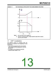
Note:
The regulator has an overload current
limiting of approximately 100 mA. During a
short circuit, the VREG is monitored. If
VREG is lower than 3.5V, the VREG will turn
off. After a recovery time of about three
milliseconds, the VREG will be checked
again. If there is no short circuit, (VREG >
3.5V) then the VREG will be switched back
on.
The regulator requires an external output bypass
capacitor for stability. See Figure 2-3 for correct capac-
ity and ESR for stable operation.
Designed for automotive applications, the regulator will
protect itself from double-battery jumps and up to +43V
load dump transients. The voltage regulator has both
short-circuit and thermal shutdown protection built-in.
The regulator has a thermal shutdown. If the thermal
protection circuit detects an over temperature
condition, and the signals TXD and RXD are LOW, or
TXD is HIGH, the regulator will shut down. The recovery
from the thermal shutdown is equal to adequate cooling
time.
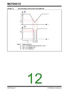
Regarding the correlation between VBB, VREG and IDD,
please refer to Figure 1-5 through 1-7. When the input
voltage (VBB) drops below the differential needed to
provide stable regulation, the output Vreg will track the
input down to approximately 3.5V, at which point the
regulator will turn off. This will allow microcontrollers
with internal POR circuits to generate a clean arming of
the Power-on Reset trip point. The MCP2021 will then
monitor VBB and turn on the regulator when Vbb is
6.0V.
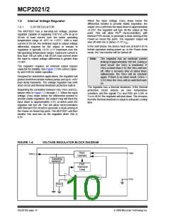
FIGURE 1-4:
VOLTAGE REGULATOR BLOCK DIAGRAM
Pass
Element
VBB
VREG
Sampling
Network
Fast
Transient
Loop
Buffer
VSS
VREF
DS22018E-page 10
© 2009 Microchip Technology Inc.

 MICROCHIP [ MICROCHIP ]