MCP2021/2
The FAULT/TXE also signals a mismatch between the
TXD input and the LBUS level. This can be used to
detect a bus contention. Since the bus exhibits a
propagation delay, the sampling of the internal
compare is debounced to eliminate false faults.
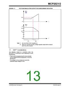
1.5.8
FAULT/TXE
Fault Detect output and Transmitter Enable input
bidirectional pin.
This pin is an open-drain output. Its state is defined as
shown in Table 1-2. The transmitter driver is disabled
whenever this pin is low (‘0’), either from an internal
fault condition or by external drive. This allows the
transmitter to be placed in an off state and still allow the
voltage regulator to operate. Refer to Table 1-1.
This pin has an internal pull-up resistor of
approximately 750 kΩ.
Note 1: The FAULT/TXE pin is true (0) whenever
the internal circuits have detected a short
or thermal excursion and have disabled
the LBUS output driver.
2: FAULT/TXE is true (0) when VREG not OK
and has disabled the LBUS output driver.
The FAULT/TXE pin sampled at a rate faster than every
10 µs.
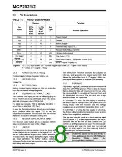
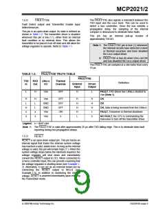
TABLE 1-2:
FAULT/TXE TRUTH TABLE
FAULT/TXE
TXD
In
RXD
Out
LINBUS
I/O
Thermal
Override
Definition
External
Input
Driven
Output
L
H
VBB
OFF
H
L
FAULT, TXD driven low, LINBUS shorted to
VBB (Note 1)
H
L
H
x
H
L
L
x
VBB
GND
GND
VBB
OFF
OFF
OFF
ON
x
H
H
H
H
L
H
H
H
L
OK
OK
OK, data is being received from the LINBUS
FAULT, Tranceiver in thermal shutdown
x
x
VBB
x
NO FAULT, the CPU is commanding the
tranceiver to turn off the transmitter driver
Legend: x = don’t care
Note 1: The FAULT/TXE is valid after approximately 25 µs after TXD falling edge. This is to eliminate false fault
reporting during bus propagation delays.
1.5.9
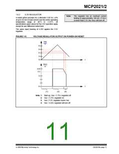
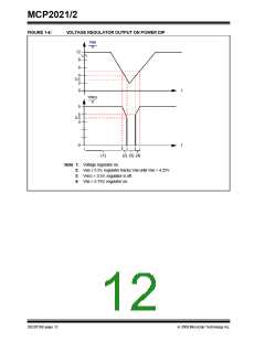
RESET
RESET is an open-drain output pin. This pin tracks an
internal signal that tracks the internal system voltage
has reached a valid, stable level. As long as the internal
voltage is valid, this pin will remain high (‘1’). When the
system voltage drops below the minimum required, the
voltage regulator will shut down and immediately
convert the RESET output to (‘0’). When connected to
a micro-controller input, this can provide a warning that
the voltage regulator is shutting down (see Example 1-
2). Alternately, it can act as an external brown-out by
connecting the RESET output to MCLR (see
Example 1-3). In addition to monitoring the internal
voltage, RESET is asserted immediately upon entering
the Powerdown mode.
© 2009 Microchip Technology Inc.
DS22018E-page 9

 MICROCHIP [ MICROCHIP ]