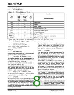
MCP2021/2
1.2
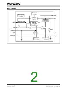
Internal Protection
1.0
DEVICE OVERVIEW
The MCP2021/2 provides a physical interface between
a microcontroller and a LIN half-duplex bus. It is
intended for automotive and industrial applications with
serial bus speeds up to 20 Kbaud.
1.2.1
ESD PROTECTION
For component-level ESD ratings, please refer to the
maximum operation specifications.
The MCP2021/2 provides a half-duplex, bidirectional
communications interface between a microcontroller
and the serial network bus. This device will translate
the CMOS/TTL logic levels to LIN level logic, and vice
versa.
1.2.2
GROUND LOSS PROTECTION
The LIN Bus specification states that the LIN pin must
transition to the recessive state when ground is
disconnected. Therefore, a loss of ground effectively
forces the LIN line to a hi-impedance level.
The LIN specification 2.0 requires that the transceiver
of all nodes in the system be connected via the LIN pin,
referenced to ground and with a maximum external
termination resistance of 510Ω from LIN bus to battery
supply. The 510Ω corresponds to 1 Master and 16
Slave nodes.
1.2.3
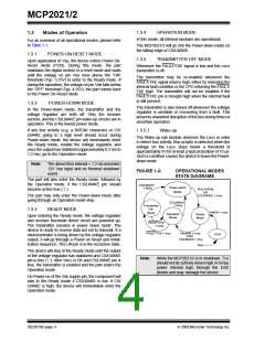
THERMAL PROTECTION
The thermal protection circuit monitors the die
temperature and is able to shut down the LIN
transmitter and voltage regulator.
There are three causes for a thermal overload. A
thermal shut down can be triggered by any one, or a
combination of, the following thermal overload
conditions.
The MCP2021-500 provides a +5V 50 mA regulated
power output. The regulator uses a LDO design, is
short-circuit-protected and will turn the regulator output
off if it falls below 3.5V. The MCP2021/2 also includes
thermal shutdown protection. The regulator has been
specifically designed to operate in the automotive
environment and will survive reverse battery connec-
tions, +43V load dump transients and double-battery
jumps. The other members of the MCP2021-330 family
output +3.3V at 50 mA with a turn-off voltage of 2.5V.
(see Section 1.6 “Internal Voltage Regulator”).
• Voltage regulator overload
• LIN bus output overload
• Increase in die temperature due to increase in
environment temperature
Driving the TXD and checking the RXD pin makes it
possible to determine whether there is a bus contention
(Rx = low, Tx = high) or a thermal overload condition
(Rx = high, Tx = low).
1.1
Optional External Protection
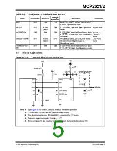
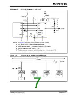
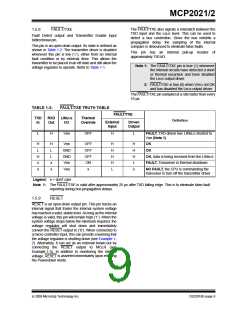
FIGURE 1-1:
THERMAL SHUTDOWN
STATE DIAGRAMS
1.1.1
REVERSE BATTERY PROTECTION
An external reverse-battery-blocking diode should be
used to provide polarity protection (see Example 1-1).
LIN bus
shorted
to VBB
Output
Overload
1.1.2
TRANSIENT VOLTAGE
Voltage
Regulator
Shutdown
PROTECTION (LOAD DUMP)
Transmitter
Shutdown
Operation
Mode
An external 43V transient suppressor (TVS) diode,
between VBB and ground, with a 50Ω transient
protection resistor (RTP) in series with the battery
supply and the VBB pin serve to protect the device from
power transients (see Example 1-1) and ESD events.
While this protection is optional, it should be
considered as good engineering practice.
Temp < SHUTDOWNTEMP
Temp < SHUTDOWN
TEMP
EQUATION 1-1:
RTP <= (VBBmin - 5.5) / 250 mA.
5.5V = VUVLO + 1.0V,
250 mA is the peak current at power-on when
VBB = 5.5V
© 2009 Microchip Technology Inc.
DS22018E-page 3

 MICROCHIP [ MICROCHIP ]