MCP2021/2
2.2
DC Specification (Continued)
Electrical Characteristics:
Unless otherwise indicated, all limits are specified for:
VBB = 6.0V to 18.0V
DC Specifications
TA = -40°C to +125°C
CLOADREG = 10 µF
Parameter
Sym
Min.
Typ.
Max.
Units
Conditions
Voltage Regulator - 3.3V
Output Voltage
VOUT
3.20
—
3.30
10
3.40
50
V
0 mA < IOUT < 50 mA
Line Regulation
ΔVOUT1
mV IOUT = 1 mA,
6.0V < VBB < 18V
Load Regulation
ΔVOUT2
—
10
50
mV 5 mA < IOUT < 50 mA
Refer to Section 1.6
“Internal Voltage
Regulator”
Quiescent Current
IVRQ
—
—
—
—
25
50
µA
dB
IOUT = 0 mA, (Note 2)
Power Supply Ripple
Reject
PSRR
1 VPP @10-20 kHz
CLOAD = 10 µf,
ILOAD = 50 mA
Output Noise Voltage
eN
—
—
100
µVRMS 10 Hz – 40 MHz
/√Hz CFILTER = 10 µf, CBP =
0.1 µf CLOAD = 10 µf,
ILOAD = 50 mA
Shutdown Voltage
VSD
VBB
2.5
6.0
—
—
2.7
V
V
See Figure 1-5
Input Voltage to Maintain
Regulation
18.0
Input Voltage to Turn Off
Output
VOFF
VON
4.0
5.5
—
—
4.5
6.0
V
V
Input Voltage to Turn On
Output
Note 1: Internal current limited. 2.0 ms maximum recovery time (RLBUS = 0Ω, TX = 0.4 VREG, VLBUS = VBB).
2: For design guidance only, not tested.
3: Node has to sustain the current that can flow under this condition; bus must be operational under this
condition.
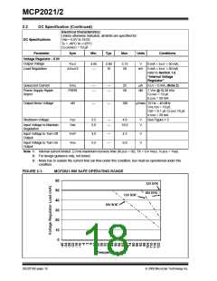
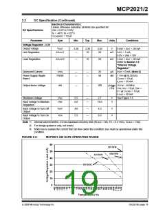
FIGURE 2-2:
MCP2021-330 SAFE OPERATING RANGE
60
50
12V DFN
18V DFN
12V SOIC
40
30
20
10
0
18V SOIC
Temperature (°C)
© 2009 Microchip Technology Inc.
DS22018E-page 19

 MICROCHIP [ MICROCHIP ]