MCP2021/2
2.2
DC Specifications
Electrical Characteristics:
Unless otherwise indicated, all limits are specified for:
VBB = 6.0V to 18.0V
DC Specifications
TA = -40°C to +125°C
CLOADREG = 10 µF
Parameter
Power
Sym
Min.
Typ.
Max.
Units
Conditions
VBB Quiescent Operating
Current
IBBQ
115
210
µA
IOUT = 0 mA,
LBUS recessive
—
—
120
90
215
190
µA
µA
VOUT = 3.3V
VBB Transmitter-off
Current
IBBTO
IBBPD
With VREG on, transmitter
off, receiver on, FAULT/
TXE = VIL, CS = VIH
—
—
95
16
210
26
µA
µA
VOUT = 3.3V
VBB Power-down Current
With VREG powered-off,
receiver on and transmitter
off, FAULT/TXE = VIH,
TXD = VIH, CS = VIL)
—
—
VBB Current with VSS
Floating
IBBNOGND
VIH
-1
1
mA VBB = 12V, GND to VBB,
VLIN = 0-18V
Microcontroller Interface
High Level Input Voltage
(TXD, FAULT/TXE)
2.0 or
(0.25VREG
+0.8)
VREG
+0.3
V
V
—
—
—
—
—
—
—
—
—
Low Level Input Voltage
(TXD, FAULT/TXE)
VIL
IIH
-0.3
-2.5
-10
0.15 VREG
High Level Input Current
(TXD, FAULT/TXE)
—
—
µA
µA
µA
V
Input voltage = 0.8*VREG
Input voltage = 0.2*VREG
Low Level Input Current
(TXD, FAULT/TXE)
IIL
Pull-up Current on Input
(TXD)
IPUTXD
VIH
-3.0
0.7VREG
-0.3
—
—
~800 kΩ internal pull-up to
VREG @ VIH = 0.7*VREG
High Level Input Voltage
(CS/LWAKE)
VBB
0.3VREG
7.0
Through a current-limiting
resistor
Low Level Input Voltage
(CS/LWAKE)
VIL
V
High Level Input Current
(CS/LWAKE)
IIH
µA
µA
µA
Input voltage = 0.8*VREG
Input voltage = 0.2*VREG
Low Level Input Current
(CS/LWAKE)
IIL
—
3.0
Pull-down Current on
Input (CS/LWAKE)
IPDCS
—
6.0
~1.3MΩ internal pull-down
to VSS @ VIH = 3.5V
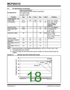
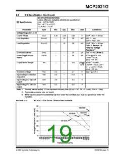
Note 1: Internal current limited. 2.0 ms maximum recovery time (RLBUS = 0Ω, TX = 0.4 VREG, VLBUS = VBB).
2: For design guidance only, not tested.
3: Node has to sustain the current that can flow under this condition; bus must be operational under this
condition.
DS22018E-page 16
© 2009 Microchip Technology Inc.

 MICROCHIP [ MICROCHIP ]