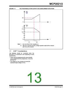
MCP2021/2
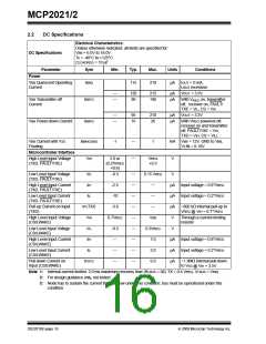
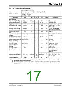
2.2
DC Specifications (Continued)
Electrical Characteristics:
Unless otherwise indicated, all limits are specified for:
VBB = 6.0V to 18.0V
DC Specifications
TA = -40°C to +125°C
CLOADREG = 10 µF
Parameter
Sym
Min.
Typ.
Max.
Units
Conditions
Bus Interface
—
—
—
—
High Level Input Voltage
Low Level Input Voltage
Input Hysteresis
VIH(LBUS)
VIL(LBUS)
VHYS
0.6 VBB
18
V
V
V
Recessive state
Dominant state
-8
—
0.4 VBB
0.175 VBB
200
VIH(LBUS) - VIL(LBUS)
Low Level Output Current
IOL(LBUS)
40
mA Output voltage = 0.1 VBB,
VBB = 12V
—
—
—
—
—
Pull-up Current on Input
IPU(LBUS)
ISC
5
50
180
200
µA
~30 kΩ internal pull-up
@ VIH (LBUS) = 0.7 VBB
Short Circuit Current
Limit
mA (Note 1)
High Level Output
Voltage
VOH(LBUS)
0.8 VBB
—
VBB
V
V
VOH(LBUS) must be at least
0.8 VBB
Low Level Output Voltage
VOLLO
(LBUS)
0.2 VBB
—
Input Leakage Current (at IBUS_PAS_DOM
the receiver during
-1
mA Driver off,
VBUS = 0V,
dominant bus level)
VBAT = 12V
—
—
Leakage Current
(disconnected from
ground)
IBUS_NO_GND
IBUS
-1
+1
10
mA
µA
GNDDEVICE = VBAT,
0V < VBUS < 18V,
VBAT = 12V
Leakage Current
(disconnected from VBAT)
—
VBAT = GND,
0 < VBUS < 18V,
TA = -40°C to +85°C
(Note 3)
50
µA
V
TA = +85°C to +125°C
Receiver Center Voltage
Slave Termination
VBUS_CNT
Rslave
0.475 VBB
20
0.5
VBB
0.525 VBB
VBUS_CNT = (VIL (LBUS) +
VIH (LBUS))/2
30
47
kΩ
Note 1: Internal current limited. 2.0 ms maximum recovery time (RLBUS = 0Ω, TX = 0.4 VREG, VLBUS = VBB).
2: For design guidance only, not tested.
3: Node has to sustain the current that can flow under this condition; bus must be operational under this
condition.
© 2009 Microchip Technology Inc.
DS22018E-page 17

 MICROCHIP [ MICROCHIP ]