ENC28J60
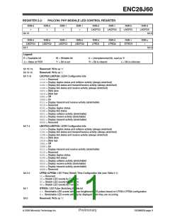
Some of the available addresses are unimplemented.
Any attempts to write to these locations are ignored
while reads return ‘0’s. The register at address 1Ah in
each bank is reserved; read and write operations
should not be performed on this register. All other
reserved registers may be read, but their contents must
not be changed. When reading and writing to registers
which contain reserved bits, any rules stated in the
register definition should be observed.
3.1
Control Registers
The Control Registers provide the main interface
between the host controller and the on-chip Ethernet
controller logic. Writing to these registers controls the
operation of the interface, while reading the registers
allows the host controller to monitor operations.
The Control Register memory is partitioned into four
banks, selectable by the bank select bits
BSEL1:BSEL0 in the ECON1 register. Each bank is
32 bytes long and addressed by a 5-bit address value.
Control registers for the ENC28J60 are generically
grouped as ETH, MAC and MII registers. Register
names starting with “E” belong to the ETH group.
Similarly, registers names starting with “MA” belong to
the MAC group and registers prefixed with “MI” belong
to the MII group.
The last five locations (1Bh to 1Fh) of all banks point to a
common set of registers: EIE, EIR, ESTAT, ECON2 and
ECON1. These are key registers used in controlling and
monitoring the operation of the device. Their common
mapping allows easy access without switching the bank.
The ECON1 and ECON2 registers are discussed later in
this section.
TABLE 3-1:
ENC28J60 CONTROL REGISTER MAP
Bank 0
Bank 1
Bank 2
Bank 3
Address
Name
ERDPTL
ERDPTH
EWRPTL
EWRPTH
ETXSTL
ETXSTH
ETXNDL
ETXNDH
ERXSTL
ERXSTH
ERXNDL
ERXNDH
ERXRDPTL
ERXRDPTH
ERXWRPTL
ERXWRPTH
EDMASTL
EDMASTH
EDMANDL
EDMANDH
EDMADSTL
EDMADSTH
EDMACSL
EDMACSH
—
Address
00h
01h
02h
03h
04h
05h
06h
07h
08h
09h
0Ah
0Bh
0Ch
0Dh
0Eh
0Fh
10h
11h
Name
EHT0
Address
00h
01h
02h
03h
04h
05h
06h
07h
08h
09h
0Ah
0Bh
0Ch
0Dh
0Eh
0Fh
10h
11h
Name
MACON1
Reserved
MACON3
MACON4
MABBIPG
—
Address
Name
MAADR5
MAADR6
MAADR3
MAADR4
MAADR1
MAADR2
EBSTSD
EBSTCON
EBSTCSL
EBSTCSH
MISTAT
—
00h
01h
02h
03h
04h
05h
06h
07h
08h
09h
0Ah
0Bh
0Ch
0Dh
0Eh
0Fh
10h
11h
12h
13h
14h
15h
16h
17h
18h
19h
1Ah
1Bh
1Ch
1Dh
1Eh
1Fh
00h
01h
02h
03h
04h
05h
06h
07h
08h
09h
0Ah
0Bh
0Ch
0Dh
0Eh
0Fh
10h
11h
12h
13h
14h
15h
16h
17h
18h
19h
1Ah
1Bh
1Ch
1Dh
1Eh
1Fh
EHT1
EHT2
EHT3
EHT4
EHT5
EHT6
MAIPGL
MAIPGH
MACLCON1
MACLCON2
MAMXFLL
MAMXFLH
Reserved
Reserved
Reserved
—
EHT7
EPMM0
EPMM1
EPMM2
EPMM3
EPMM4
EPMM5
EPMM6
EPMM7
EPMCSL
EPMCSH
—
—
—
—
—
Reserved
Reserved
MICMD
—
—
—
12h
13h
14h
15h
16h
17h
18h
19h
1Ah
1Bh
1Ch
1Dh
1Eh
1Fh
12h
13h
14h
15h
16h
17h
18h
19h
1Ah
1Bh
1Ch
1Dh
1Eh
1Fh
EREVID
—
—
EPMOL
EPMOH
Reserved
Reserved
ERXFCON
EPKTCNT
Reserved
EIE
MIREGADR
Reserved
MIWRL
—
ECOCON
Reserved
EFLOCON
EPAUSL
EPAUSH
Reserved
EIE
MIWRH
MIRDL
—
MIRDH
Reserved
EIE
Reserved
EIE
EIR
EIR
EIR
EIR
ESTAT
ESTAT
ECON2
ECON1
ESTAT
ESTAT
ECON2
ECON1
ECON2
ECON2
ECON1
ECON1
DS39662B-page 12
Preliminary
© 2006 Microchip Technology Inc.

 MICROCHIP [ MICROCHIP ]