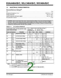
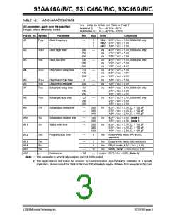
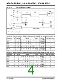
93AA46A/B/C, 93LC46A/B/C, 93C46A/B/C
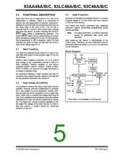
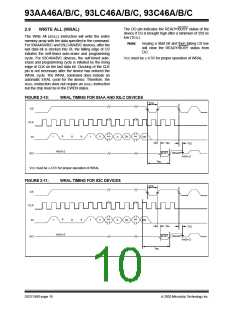
The DO pin indicates the READY/BUSY status of the
2.4
ERASE
device if CS is brought high after a minimum of 250 ns
low (TCSL). DO at logical ‘0’ indicates that programming
is still in progress. DO at logical ‘1’ indicates that the
register at the specified address has been erased and
the device is ready for another instruction.
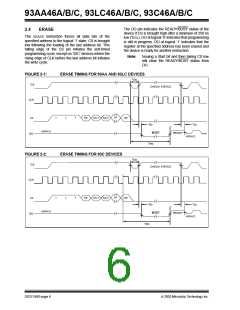
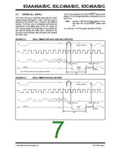
The ERASE instruction forces all data bits of the
specified address to the logical ‘1’ state. CS is brought
low following the loading of the last address bit. This
falling edge of the CS pin initiates the self-timed
programming cycle, except on ‘93C’ devices where the
rising edge of CLK before the last address bit initiates
the write cycle.
Note:
Issuing a Start bit and then taking CS low
will clear the READY/BUSY status from
DO.
FIGURE 2-1:
ERASE TIMING FOR 93AA AND 93LC DEVICES
TCSL
CS
CHECK STATUS
CLK
DI
1
1
AN
AN-1 AN-2
A0
•••
1
TSV
TCZ
HIGH-Z
BUSY
READY
DO
HIGH-Z
TWC
FIGURE 2-2:
ERASE TIMING FOR 93C DEVICES
TCSL
CS
CHECK STATUS
CLK
DI
1
1
AN
AN-1 AN-2
A0
•••
1
TSV
TCZ
HIGH-Z
BUSY
READY
DO
HIGH-Z
TWC
DS21749D-page 6
2003 Microchip Technology Inc.

 MICROCHIP [ MICROCHIP ]